Superjunction device structure and method for fabricating same

A technology of superjunction device and column structure, applied in the field of superjunction device structure and its preparation, can solve problems such as uneven defects in the superjunction drift region, and achieve a technology suitable for large-scale production, optimized reverse recovery characteristics and simple process. Effect

Inactive Publication Date: 2019-09-17
上海功成半导体科技有限公司
View PDF5 Cites 1 Cited by
  • Summary
  • Abstract
  • Description
  • Claims
  • Application Information

AI Technical Summary

Problems solved by technology

[0005] In view of the above-mentioned shortcomings of the prior art, the object of the present invention is to provide a super junction device structure and its preparation method, which is used to solve the problem of uneven introduction of defects in the super junction drift region in the prior art

Method used


Image

  • Superjunction device structure and method for fabricating same
  • Superjunction device structure and method for fabricating same
  • Superjunction device structure and method for fabricating same

Examples


Embodiment 1

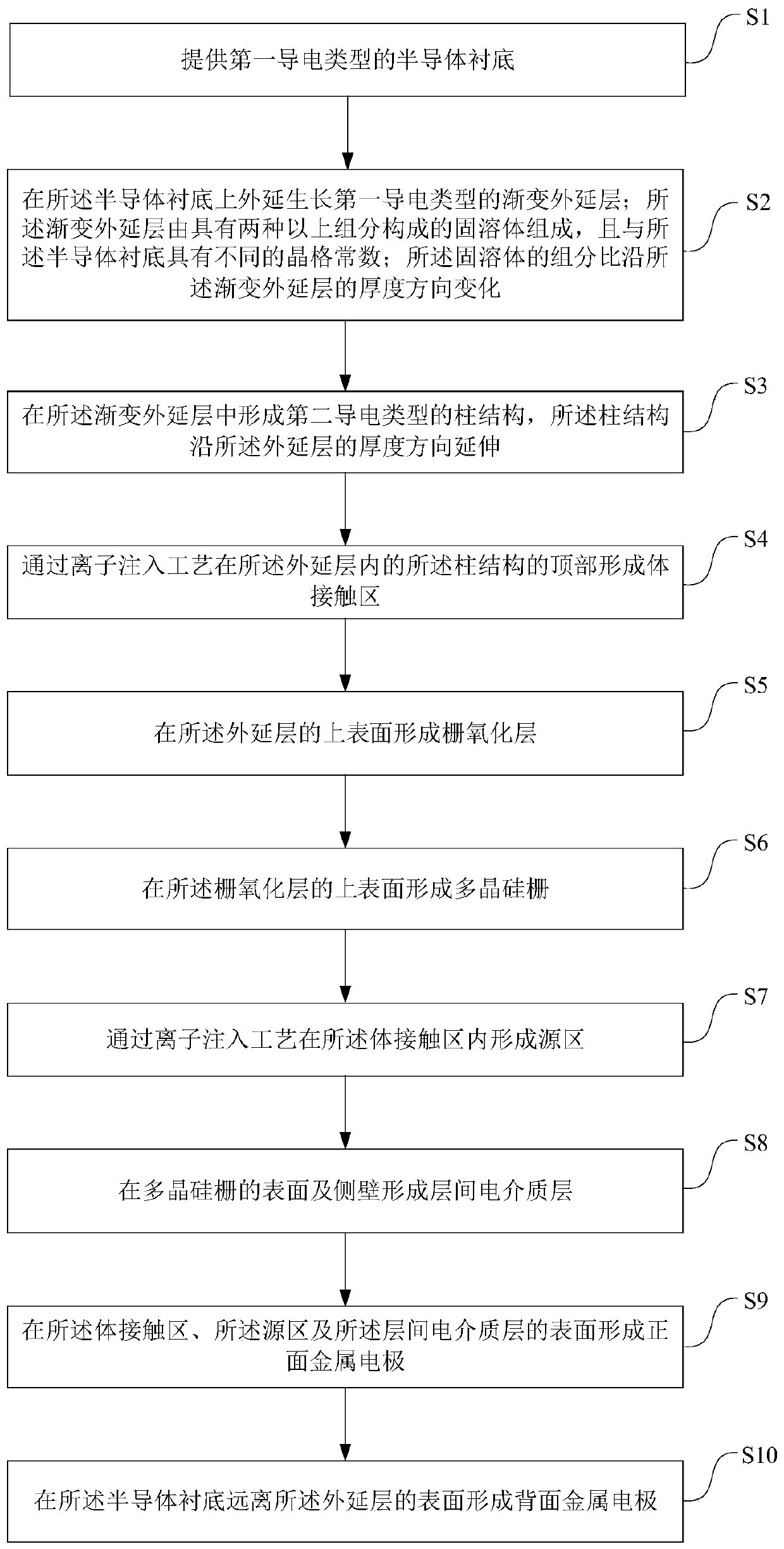
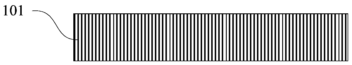
[0067] see Figure 1 to Figure 12 , the invention provides a method for preparing a superjunction device structure, comprising the following steps:

[0068] 1) providing a semiconductor substrate 101 of the first conductivity type;

[0069] 2) Epitaxially growing a graded epitaxial layer 102 of the first conductivity type on the semiconductor substrate 101; the graded epitaxial layer 102 is composed of a solid solution composed of two or more components, and has a different The lattice constant; the composition ratio of the solid solution changes along the thickness direction of the graded epitaxial layer 102;

[0070] 3) Forming a column structure 103 of the second conductivity type in the graded epitaxial layer 102 , and the column structure 103 extends along the thickness direction of the graded epitaxial layer 102 .

[0071] In step 1), see figure 1 The S1 step and figure 2 , providing a semiconductor substrate 101 of the first conductivity type. figure 2 is a schem...

Embodiment 2

[0110] This embodiment provides a superjunction device structure and its preparation method. Compared with Embodiment 1, the difference of this embodiment is that the germanium-silicon composition ratio of the germanium-silicon material constituting the pillar structure can also vary with the pillar structure. The depth direction changes gradually.

[0111] As an example, when the thickness of the graded epitaxial layer is 50 microns and the depth of the column structure is 42 microns, in the thickness direction, the atomic percentage of germanium is from 0.5% of the lower surface of the graded epitaxial layer 102 Gradually increase to 5% of the upper surface of the graded epitaxial layer 102 . In order to match the change of germanium content in the graded epitaxial layer, the germanium content in the column structure can also be set to gradually change along the depth direction of the column structure. For example, the germanium content is lower at the bottom of the pillar ...


PUM

PropertyMeasurementUnit
thicknessaaaaaaaaaa
thicknessaaaaaaaaaa
thicknessaaaaaaaaaa

Abstract

The invention provides a superjunction device structure and a method for fabricating the same. The superjunction device structure comprises a first conductivity type of semiconductor substrate; a first conductivity type of graded epitaxial layer formed on the semiconductor substrate, composed of a solid solution having more than two components, and having a different lattice constant from the semiconductor substrate, wherein the component ratio of the solid solution varies in the thickness direction of the graded epitaxial layer; and a second conductivity type of pillar structure formed in the graded epitaxial layer and extending in the thickness direction of the epitaxial layer. The lattice defect is uniformly controllable in the thickness direction of the epitaxial layer by growing the graded epitaxial layer in which the solid solution components vary in the thickness direction and which has a different lattice constant from the semiconductor substrate. The reverse recovery characteristic of a device is optimized to realize a purpose of rapidly reducing carriers during the turn-off phase of the device. The superjunction device structure is simple in process, low in cost, and suitable for mass production.

Description

technical field [0001] The invention relates to the field of semiconductor integrated circuit manufacturing, in particular to a superjunction device structure and a preparation method thereof. Background technique [0002] The super junction device (super junction) is a semiconductor power device with unique advantages. It has high withstand voltage performance and low on-resistance, breaking the traditional silicon-based high-voltage device that cannot have both high withstand voltage and low resistance. limits. [0003] At present, in typical applications of power devices such as half-bridge and full-bridge, the switching speed of super-junction power devices is greatly limited due to the limitation of the reverse recovery characteristics of parasitic diodes. In order to optimize the reverse recovery characteristics of superjunction devices to reduce power consumption and increase device reliability, a more effective method is to introduce defects in the drift region to i...

Claims


Application Information

Patent Timeline
Patent Type & Authority Applications(China)
IPC IPC(8): H01L29/06H01L29/78H01L21/336
CPCH01L29/0634H01L29/78H01L29/66477
Inventor 徐大朋梁欢黄肖艳薛忠营罗杰馨柴展
Owner 上海功成半导体科技有限公司
Why Eureka
Try Eureka