
High-heat-resistant packaging substrate

A packaging carrier, high heat-resistant technology, applied in the direction of electrical components, electric solid devices, circuits, etc., can solve the problems of self-encapsulation substrates such as glass and chip differences, and packaging structure thickness reduction obstacles, etc., to improve heat resistance. , increase the service life, improve the effect of cooling efficiency

Inactive Publication Date: 2019-09-20
江门建滔电子发展有限公司
View PDF4 Cites 4 Cited by
  • Summary
  • Abstract
  • Description
  • Claims
  • Application Information

AI Technical Summary

Problems solved by technology

If the thickness of the core dielectric layer cannot be effectively reduced, it will inevitably cause a great obstacle in reducing the thickness of the packaging structure
[0003] In the existing packaging manufacturing process, due to the large difference between the thermal expansion coefficient of the chip and the packaging substrate, the chip cannot form a good bond with the packaging substrate, so that the chip or the bump located between the chip and the packaging substrate may automatically package glass on substrate
In addition, as the integration of integrated circuits increases, due to the thermal expansion coefficient mismatch between the chip and the packaging substrate and the insulating layer, the thermal stress and warpage caused by it are becoming more and more serious, resulting in the chip and packaging substrate drop in reliability

Method used


Image

  • High-heat-resistant packaging substrate

Examples


Embodiment 1

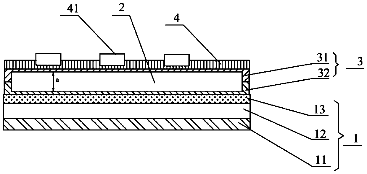
[0016] A high heat-resistant packaging carrier board, including a substrate 1, a circuit board 2, a high heat-resistant insulating layer 4, a patterned conductive layer 41 and a solder mask 3, the substrate 1 is sequentially composed of a release layer 13, A dielectric layer 12 and a copper foil layer 11 are formed. The circuit board 2 is located on the substrate 1 and is in contact with the release layer 13 of the substrate 1. A high heat-resistant insulating layer 4 is provided above the circuit board 2. A patterned conductive layer 41 is arranged on the upper part of the high heat-resistant insulating layer 4. Electronic components are arranged in the patterned conductive layer 41, and the electronic components are suitable for being arranged on the high heat-resistant insulating layer 4. The high heat-resistant The thermal expansion coefficient of the insulating layer 4 is between that of the substrate 1 and the electronic components. The solder resist layer 3 includes a fi...

Embodiment 2

[0021] A high heat-resistant packaging carrier board, including a substrate 1, a circuit board 2, a high heat-resistant insulating layer 4, a patterned conductive layer 41 and a solder mask 3, the substrate 1 is sequentially composed of a release layer 13, A dielectric layer 12 and a copper foil layer 11 are formed. The circuit board 2 is located on the substrate 1 and is in contact with the release layer 13 of the substrate 1. A high heat-resistant insulating layer 4 is provided above the circuit board 2. A patterned conductive layer 41 is arranged on the upper part of the high heat-resistant insulating layer 4. Electronic components are arranged in the patterned conductive layer 41, and the electronic components are suitable for being arranged on the high heat-resistant insulating layer 4. The high heat-resistant The thermal expansion coefficient of the insulating layer 4 is between that of the substrate 1 and the electronic components. The solder resist layer 3 includes a fi...


PUM


Abstract

The invention discloses a high-heat-resistant packaging substrate. The high-heat-resistant packaging substrate comprises a base plate, a circuit board, a high-heat-resistant insulating layer, a patterned conductive layer and an anti-welding layer, wherein the circuit board is positioned on the upper surface of the base plate; the high-heat-resistant insulating layer is arranged above the circuit board; the patterned conductive layer is arranged at the upper portion of the high-heat-resistant insulating layer; an electronic element is arranged in the patterned conductive layer; and a thermal expansion coefficient of the high-heat-resistant insulating layer is between the thermal expansion coefficients of the base plate and the electronic element. The thermal expansion coefficient difference among the electronic element, the high-heat-resistant insulating layer and the base plate of the high-heat-resistant packaging substrate is gradually reduced, so that the phenomena that the electronic element falls off and is stripped can be avoided, and the service life of the packaging substrate is prolonged; the high-heat-resistant insulating layer is adopted, so that the heat-resistant strength of the substrate can be improved; the thickness of the circuit board is small, so that the subsequently finished packaging structure has relatively small packaging thickness, and the heat dissipation efficiency of the packaging substrate is improved; and the packaging substrate is suitable for industrial large-scale production.

Description

technical field [0001] The invention relates to the technical field of packaging carrier boards, in particular to a high heat-resistant packaging carrier board. Background technique [0002] Chip packaging is to provide appropriate signal paths, heat conduction paths, and structural protection for the chip. The traditional wire bonding technology usually uses a lead frame as a chip carrier. As the contact density of the chip gradually increases, the lead frame can no longer provide a higher contact density. Therefore, a package carrier with a high contact density can be used instead, and the chip is packaged into the package through conductive media such as metal wires or bumps. carrier board. Usually, the core dielectric layer is used as the core material in the manufacture of the packaging substrate, and the multi-layer patterned circuit layer and the patterned dielectric layer are stacked alternately by using the full additive method, semi-additive method, subtractive m...

Claims


Application Information

Patent Timeline
Patent Type & Authority Applications(China)
IPC IPC(8): H01L23/367H01L23/498
CPCH01L23/367H01L23/49822H01L23/49838
Inventor 周培峰
Owner 江门建滔电子发展有限公司
Learn More