SMT chip defect detection system and method

A chip defect and detection method technology, which is applied in the direction of optical testing flaws/defects, measuring devices, instruments, etc., can solve problems such as high labor costs, poor quality inspection results, and operator mental fatigue, so as to reduce the difficulty of detection and improve detection. Efficiency and detection quality, effect of improving working conditions

Inactive Publication Date: 2019-10-15
DONGHUA UNIV
View PDF3 Cites 7 Cited by
  • Summary
  • Abstract
  • Description
  • Claims
  • Application Information

AI Technical Summary

Problems solved by technology

This detection method not only requires a lot of labor, but also the workers on the assembly line have to repeat the same quality inspection content, which is easy to cause mental fatigue of the operator
This detection method has high labor cost, low quality inspection efficiency, and poor quality inspection effect

Method used


Image

  • SMT chip defect detection system and method
  • SMT chip defect detection system and method

Examples


Embodiment

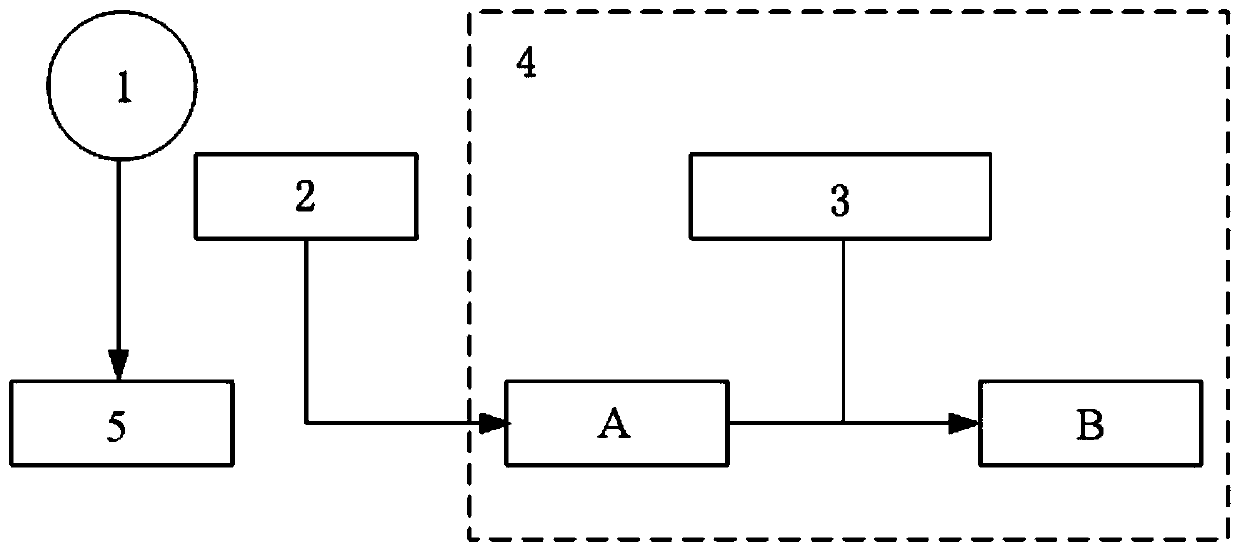
[0031] Such as figure 1 Shown, for a kind of SMT chip defect detection system provided by the present invention, it comprises:

[0032] A ring-shaped LED light source 1 for illuminating the SMT chip 5;

[0033] An imaging system 2, configured to acquire an image and transmit the acquired image signal A to an image processing system 3;

[0034] An image processing system 3, configured to process the image signal A acquired by the imaging system 2;

[0035] The industrial computer 4 is used to intuitively output the image signal A processed by the image processing system 3 in the form of human-computer interaction. The industrial computer 4 includes the port of the imaging system 2, the image processing system 3 and the human-computer interaction interface, wherein the human-computer interaction interface can execute manually written image processing codes to output the detection result B intuitively.

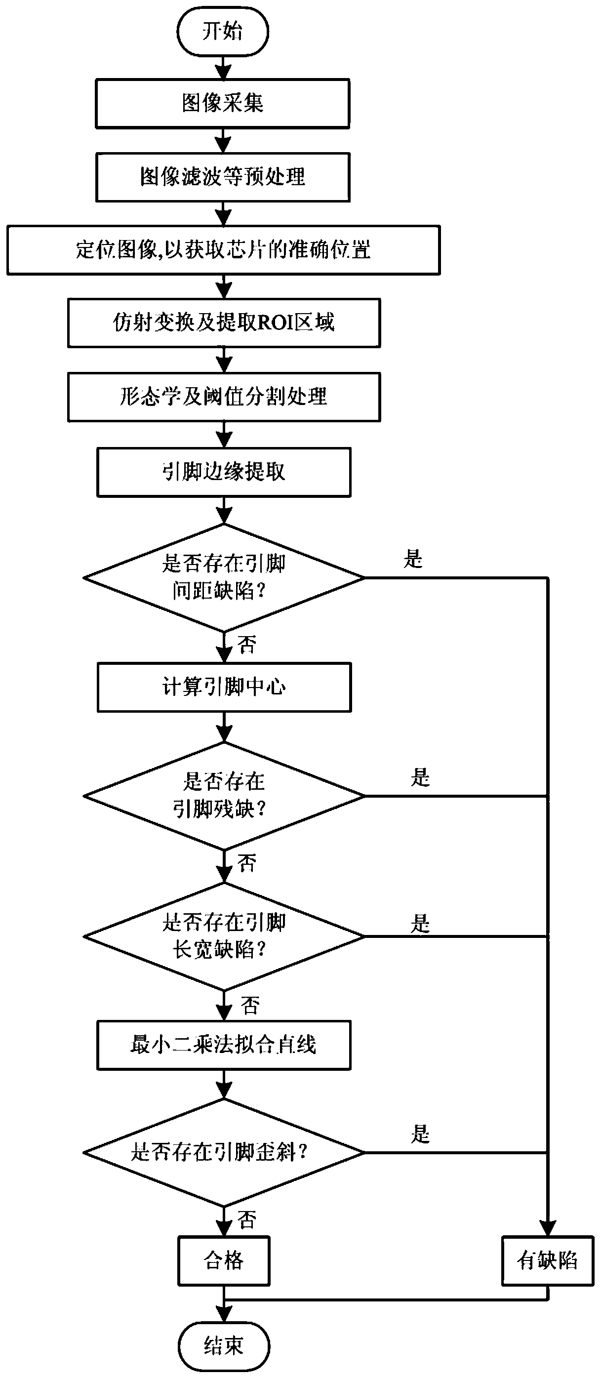
[0036] A kind of SMT chip defect detection method, such as figure 2 As ...


PUM


Abstract

The invention discloses a SMT chip defect detection system and method. The system comprises an annular LED light source, an image acquisition system, an image processing system and an industrial personal computer. The detection method comprises the following steps: the image acquisition system transmits an acquired image signal to the image processing system; the image processing system processesan original image, extracts a pin image, and measures the related data of the pin; the related data of the pin is compared with the standard value and judged; and the related data of the pin and the judgment result are visually displayed in a human-machine interaction way, and a detection result is output. The vision detection of the SMT chip is realized, the detection difficulty is reduced, the working condition of the detection worker is improved, and the detection efficiency and the detection quality of the SMT chip are improved.

Description

technical field [0001] The invention relates to an SMT chip defect detection system and method, belonging to the technical field of semiconductor chip defect detection. Background technique [0002] At present, in most semiconductor chip production workshops, the SMT chips packaged and molded by the packaging machine are transported by the conveyor belt to the quality inspection line for quality defect detection. At present, manual methods are generally used in the workshop to detect the quality of SMT chip pins. The content of the detection includes the number of pins, length and width, spacing, and flatness. This detection method not only requires a lot of labor, but also the workers on the assembly line have to repeat the same quality inspection content continuously, which is easy to cause mental fatigue of the operator. This detection method has high labor cost, low quality inspection efficiency, and poor quality inspection effect. Contents of the invention [0003] ...

Claims


Application Information

Patent Timeline
Patent Type & Authority Applications(China)
IPC IPC(8): G01N21/88G01B11/02G01B11/14G01B11/30
CPCG01B11/02G01B11/14G01B11/30G01N21/8851G01N2021/8883G01N2021/8887
Inventor 费胜巍范晞
Owner DONGHUA UNIV
Why Eureka
Try Eureka