Supercharge Your Innovation With Domain-Expert AI Agents!

HEMT structure and manufacturing method thereof

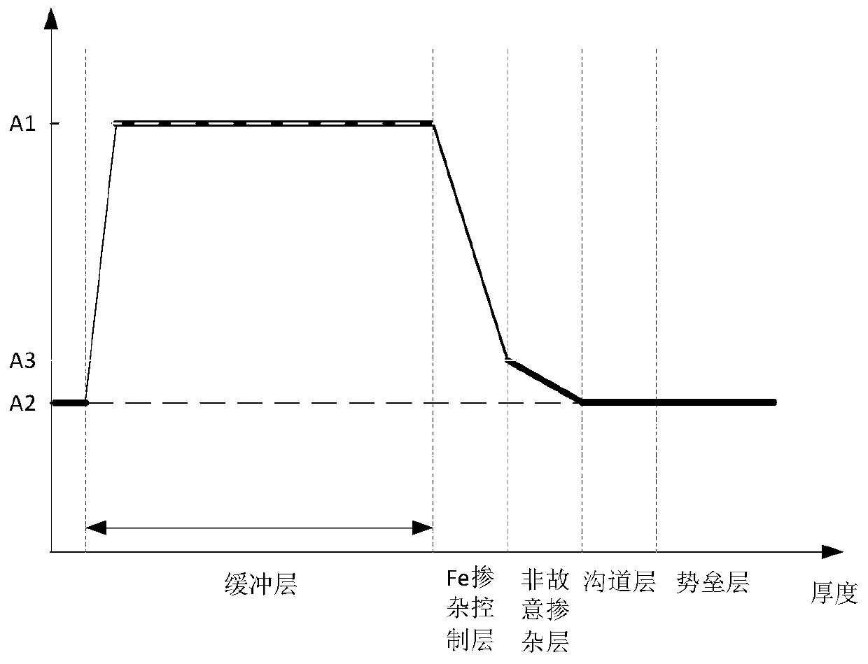
A technology of control layer and buffer layer, which is applied in semiconductor/solid-state device manufacturing, electrical components, circuits, etc., can solve the problems of thick iron-doped layer thickness, limitation of device structure design, uneven distribution of iron-doped layer concentration, etc. Achieve the effect of reducing thickness, increasing attenuation rate and improving insulation effect

Active Publication Date: 2019-10-15
SUZHOU HAN HUA SEMICON CO LTD
View PDF3 Cites 0 Cited by
  • Summary
  • Abstract
  • Description
  • Claims
  • Application Information

AI Technical Summary

Problems solved by technology

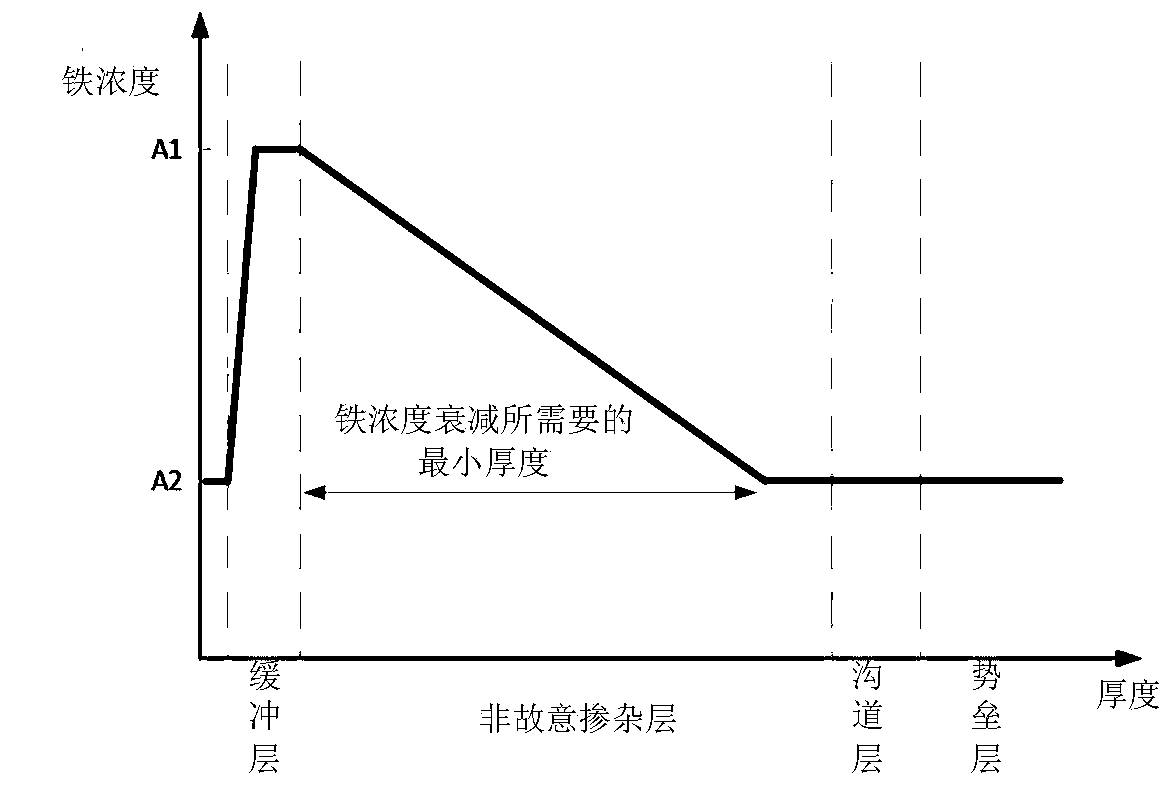
This will lead to the following problems: 1) the thickness of the iron-doped layer is thick, which will bring great restrictions to the design of the device structure; in addition, the thicker GaN layer is not conducive to the heat dissipation of the device; 2) the iron-doped layer The concentration distribution of the impurity layer is not uniform: the difference between the iron concentration at the beginning stage and the iron concentration at the end stage can reach one to two orders of magnitude, resulting in insufficient insulation of the GaNbuffer layer

Method used


Image

  • HEMT structure and manufacturing method thereof
  • HEMT structure and manufacturing method thereof
  • HEMT structure and manufacturing method thereof

Examples


Embodiment Construction

[0027] The HEMT structure proposed by the present invention and its manufacturing method will be further described in detail below in conjunction with the accompanying drawings and specific embodiments. Advantages and features of the present invention will be apparent from the following description and claims. It should be noted that all the drawings are in a very simplified form and use imprecise scales, and are only used to facilitate and clearly assist the purpose of illustrating the embodiments of the present invention.

[0028] In the present invention, in "a layer formed on another layer", it may mean that a layer is formed on another layer, but not necessarily that the layer is in direct physical or electrical contact with another layer (for example, there may be one or more other layers in between). However, in some embodiments, "formed on" may mean that a layer is in direct physical contact with at least a portion of the top surface of another layer.

[0029] An emb...


PUM


Abstract

The invention relates to an HEMT structure, which includes a substrate, a buffer layer with iron doping located on the substrate, a doping control layer located on the buffer layer, an unintentional doped layer located on the doping control layer, and a channel layer and a barrier layer located on the unintentional doped layer in turn. According to the HEMT structure and a manufacturing method thereof presented by the application, through the introduction of the doping control layer, the attenuation rate of the doping elements is increased, the thickness of the doped layer is reduced, and theinsulation effect of the buffer layer is improved.

Description

technical field [0001] The invention relates to the technical field of semiconductor manufacturing, in particular to a HEMT structure and a manufacturing method thereof. Background technique [0002] As a representative of the third-generation semiconductor materials, gallium nitride (GaN) has many excellent characteristics, such as high critical breakdown electric field, high electron mobility, high two-dimensional electron gas concentration, and good high temperature working ability. Gallium nitride-based third-generation semiconductor devices, such as high electron mobility transistors (HEMTs) and heterostructure field effect transistors (HFETs), have been applied, especially in fields requiring high power and high frequency such as radio frequency and microwave has obvious advantages. [0003] In conventional HEMTs, in order to achieve the purpose of growing a high-resistance GaN layer to reduce the leakage of the buffer layer (buffer), doping (usually iron) is often pe...

Claims


Application Information

Patent Timeline
Patent Type & Authority Applications(China)
IPC IPC(8): H01L29/06H01L29/778H01L21/335
CPCH01L29/0684H01L29/66462H01L29/778
Inventor 倪贤锋范谦孙培浩何伟
Owner SUZHOU HAN HUA SEMICON CO LTD
Features
  • R&D
  • Intellectual Property
  • Life Sciences
  • Materials
  • Tech Scout
  • Unparalleled Data Quality
  • Higher Quality Content
  • 60% Fewer Hallucinations
Learn More