Surface-mount packaging equipment for semiconductor epitaxial film

A technology of epitaxial film and packaging equipment, applied in semiconductor/solid-state device manufacturing, electrical components, circuits, etc., can solve the problems of difficult removal of epitaxial film, pin positioning deviation, pin flying out, etc., to reduce the epitaxial rate of chip film , The effect of stable heat dissipation and reduced workload

Active Publication Date: 2019-10-22
苏州施密科微电子设备有限公司
View PDF7 Cites 6 Cited by
  • Summary
  • Abstract
  • Description
  • Claims
  • Application Information

AI Technical Summary

Problems solved by technology

[0002] Nowadays, electronic chips are ushering in an era of high development, and the use of microelectronic packaging technology in the field of semiconductor packaging is becoming more and more mature. Replaced by sub-packaging technologies such as PQFN and BGA, on the basis of a large number of three-dimensional packaging, the semiconductor motherboard or each base unit is performing film lamination. Due to the secondary lamination after bonding, cutting is originally performed after film lamination The docile film will spread and extend outward due to extrusion, and it will be baked after the second lamination. At the s

Method used


Image

  • Surface-mount packaging equipment for semiconductor epitaxial film
  • Surface-mount packaging equipment for semiconductor epitaxial film
  • Surface-mount packaging equipment for semiconductor epitaxial film

Examples


Example Embodiment

[0028] The technical solutions in the embodiments of the present invention will be clearly and completely described below in conjunction with the accompanying drawings in the embodiments of the present invention. Obviously, the described embodiments are only some, not all, embodiments of the present invention. Based on the embodiments of the present invention, all other embodiments obtained by those of ordinary skill in the art without creative efforts shall fall within the protection scope of the present invention.

[0029] Those of ordinary skill in the art will recognize that "upper end", "lower end",

[0030] Orientation terms such as "outer" and "inner" are descriptive terms for the drawings, and do not represent limitations on the scope of protection defined in the claims.

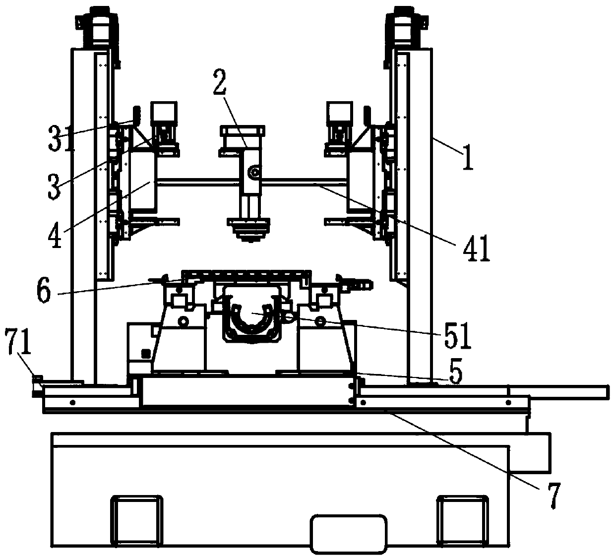
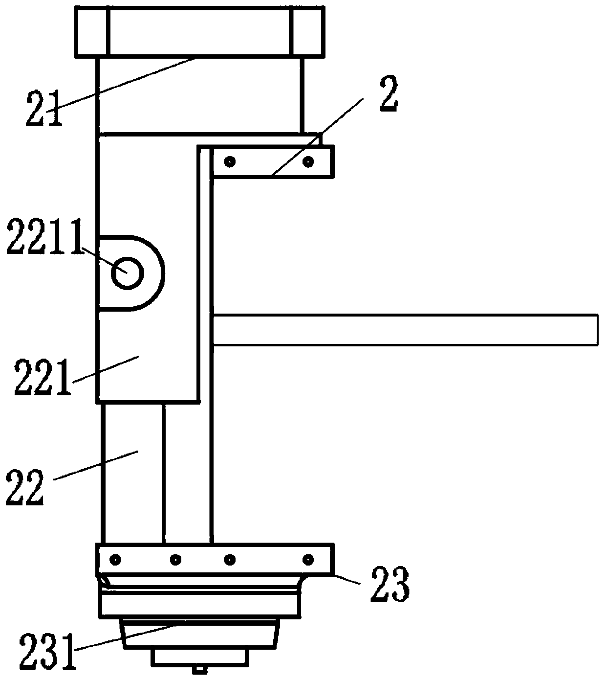
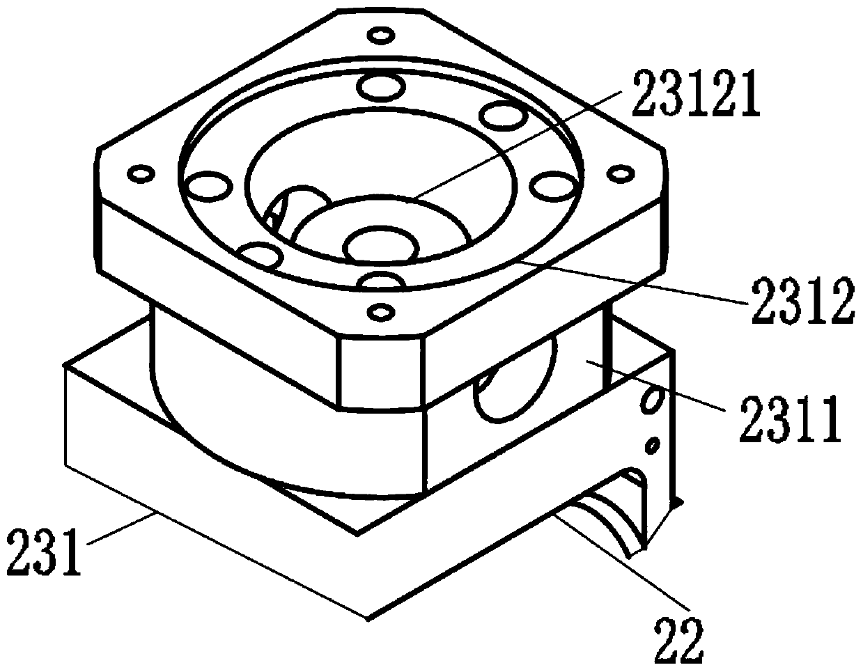
[0031] see Figure 1-2 , the present invention provides a technical solution: a semiconductor epitaxial thin film chip packaging equipment, including a main frame support platform 1, a packaging exe...


PUM


Abstract

The invention discloses surface-mount packaging equipment for a semiconductor epitaxial film, which comprises main framework supporting platforms, a packaging execution module and a packaging disc group, wherein the main framework supporting platforms are symmetrically arranged by taking a saddle as the axis, each pneumatic rod is in pneumatic connection with a second connecting rod extending in the horizontal transverse direction, and the packaging execution module is slidably installed on the second connecting rod; and the packaging execution module is an active mechanism module which is used for operating a pasting process between an integrated circuit chip transferred at the upper working section and a packaging substrate or a pin frame. The surface-mount packaging equipment for the semiconductor epitaxial film adopts transistor inner shape grid array packaging, is different from packaging modes such as transistor outer shape packaging and pin grid array packaging, has the advantages of reducing the epitaxial rate of a chip film and reducing the error rate of chip packaging, and adopts a point contact cutting mode of linear cutting to cut off lead feet, pins or redundant upperextending film tissues at one time, so that the destructiveness is low, the cutting speed is higher, and the efficiency is higher.

Description

technical field [0001] The invention relates to semiconductor packaging equipment, in particular to semiconductor epitaxial thin film chip packaging equipment. Background technique [0002] Nowadays, electronic chips are ushering in an era of high development, and the use of microelectronic packaging technology in the field of semiconductor packaging is becoming more and more mature. Replaced by sub-packaging technologies such as PQFN and BGA, on the basis of a large number of three-dimensional packaging, the semiconductor motherboard or each base unit is performing film lamination. Due to the secondary lamination after bonding, cutting is originally performed after film lamination The docile film will spread and extend outward due to extrusion, and it will be baked after the second lamination. At the same time, in order to obtain the best chip placement rate, the back of the IC chip must not only be coated first, but also need to be planted on the carrier. This leads to th...

Claims


Application Information

Patent Timeline
IPC IPC(8): H01L21/67
CPCH01L21/67092H01L21/67121H01L21/67144
Inventor 陈海吟
Owner 苏州施密科微电子设备有限公司
Why Eureka
Try Eureka