MEMS device and preparation method thereof

A technology of devices and cuboids, which is applied in the field of MEMS devices and its preparation, can solve the problems of increasing the fluctuation range of device sensitivity and signal-to-noise ratio, the relatively large application of the vibrating film, and the loss of the vibrating film, so as to increase the effective vibration area, Improve the sensitivity and signal-to-noise ratio, reduce the effect of amplitude

Active Publication Date: 2019-10-22
SEMICON MFG INT (SHANGHAI) CORP +1
View PDF8 Cites 0 Cited by
  • Summary
  • Abstract
  • Description
  • Claims
  • Application Information

AI Technical Summary

Problems solved by technology

[0004] However, since the vibrating membrane is equivalent to a thin film in motion, a relatively large amplitude will be generated in a relatively small effective vibration area, and the large vibration amplitude will cause the sensitivity of the device and the fluctuation range of the signal-to-noise ratio to increase, and in some Mechanical reliability tests will exert relatively large force on the vibrating membrane, such as air pressure test or mechanical impact test, which may easily cause loss or damage of the vibrating membrane

Method used


Image

  • MEMS device and preparation method thereof
  • MEMS device and preparation method thereof
  • MEMS device and preparation method thereof

Examples


preparation example Construction

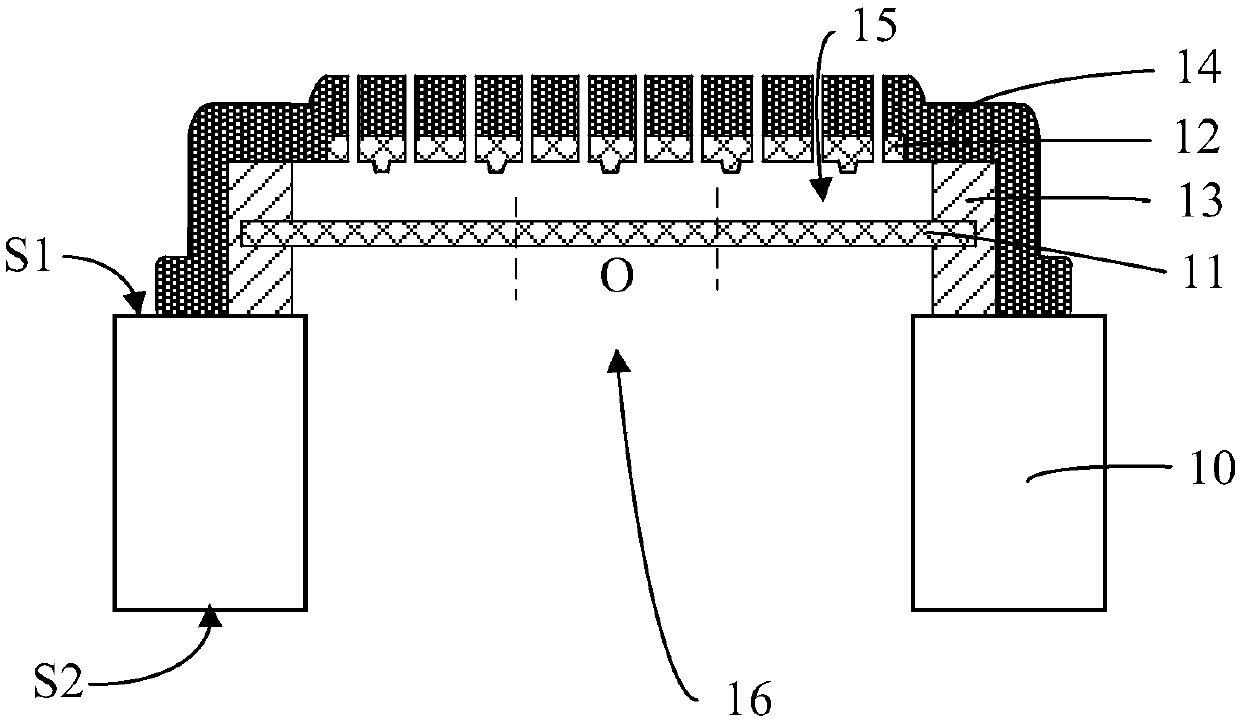
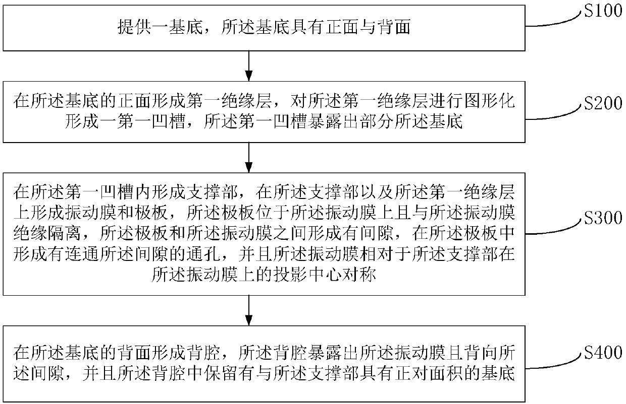
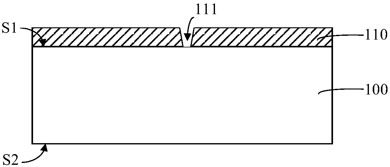
[0052] In view of the above problems, the inventors of the present application have proposed a method for preparing a MEMS device, including: providing a base, the base has a front and a back; forming a first insulating layer on the front of the base, and insulating the first The layer is patterned to form a first groove, and the first groove exposes part of the substrate; a support portion is formed in the first groove, and a support portion is formed on the support portion and the first insulating layer. a vibrating membrane and a pole plate, the pole plate is located on the vibrating membrane and is insulated from the vibrating membrane, a gap is formed between the pole plate and the vibrating membrane, and a communication channel is formed in the pole plate The through hole of the gap, and the vibrating membrane is symmetrical with respect to the projection center of the supporting part on the vibrating membrane; a back cavity is formed on the back of the substrate, the bac...


PUM


Abstract

The invention provides an MEMS device and a preparation method thereof. The MEMS device is characterized in that: a vibrating diaphragm is formed on the front surface of a substrate; a support part isformed between the vibrating diaphragm and the substrate; the vibrating diaphragm is symmetrical relative to the projection center of the supporting part on the vibrating diaphragm; a back cavity isformed on the back surface of the substrate; the back cavity exposes the vibrating diaphragm and is back to the gap, and remains the substrate, having an area opposite to the supporting part, in the back cavity as a supporting substrate of the supporting part; and when the vibrating diaphragm vibrates, the vibrating diaphragm vibrates at the middle position between the edge and the center of the vibrating diaphragm. Compared with the prior art, the effective vibration area is increased, so that the sensitivity and the signal-to-noise ratio of the MEMS device are improved, and the vibration amplitude is reduced, and the fluctuation range of the sensitivity and the signal-to-noise ratio is reduced; and meanwhile, the force applied to the vibrating diaphragm in a mechanical reliability test is reduced, so that the reliability of the MEMS device is improved.

Description

technical field [0001] The invention relates to the technical field of semiconductors, in particular to a MEMS device and a preparation method thereof. Background technique [0002] MEMS (Micro-Electro-Mechanical System, Micro-Electro-Mechanical System) technology refers to a micro-system that can integrate mechanical components, drive components, optical systems, and electronic control systems into a whole. It uses microelectronics technology and micromachining technology ( Such as silicon body micromachining, silicon surface micromachining, wafer bonding, etc.) combined manufacturing process, to produce a variety of excellent performance, low price, miniaturized sensors (such as inertial sensors, pressure sensors, acceleration sensors, etc.), execution drives, drives and microsystems. [0003] Existing MEMS devices generally include a base, the base has a front and a back, and the base has a back cavity that runs through the front and the back, a vibrating membrane is for...

Claims


Application Information

Patent Timeline
Patent Type & Authority Applications(China)
IPC IPC(8): H04R31/00H04R19/00
CPCH04R19/005H04R31/003H04R2201/003H04R2231/001
Inventor 李鑫郭亮良
Owner SEMICON MFG INT (SHANGHAI) CORP
Why Eureka
Try Eureka