An order-disorder phase transition-based shape memory method for semiconductor materials

A technology of semiconductors and ordered phases, applied in chemical instruments and methods, inorganic chemistry, electrical components, etc., can solve problems that limit the application of shape memory materials

Active Publication Date: 2020-08-07
ZHEJIANG UNIV
View PDF2 Cites 0 Cited by
  • Summary
  • Abstract
  • Description
  • Claims
  • Application Information

AI Technical Summary

Problems solved by technology

This also greatly limits the application of shape memory materials in the fields of microelectronics and electronic information.

Method used


Image

  • An order-disorder phase transition-based shape memory method for semiconductor materials
  • An order-disorder phase transition-based shape memory method for semiconductor materials
  • An order-disorder phase transition-based shape memory method for semiconductor materials

Examples


Embodiment 1

[0034] Embodiment 1: the shape memory effect of nanowire section sample:

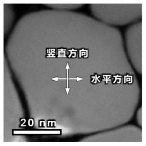
[0035] The first step is to prepare Ag by using focused ion beam micro-nano processing instrument 2 S nanowire cross-section sample and transferred to the heating chip, as figure 2 shown.

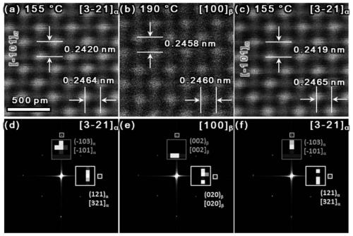
[0036] In the second step, the sample is heated to 10-20°C below the phase transition point of the sample (due to the nanoscale Ag 2 The α-β phase transition point of S decreases as its size decreases. At the same time, considering the convenience of rapid temperature rise across its phase transition point, the low-temperature phase holding temperature is usually 130-160 ° C. The preferred temperature for nanomaterials with a size of 45 nm is 155°C).

[0037] In the third step, the sample is rapidly heated until the phase transition is completed and becomes the BCC phase (due to the nanoscale Ag 2 The β-α phase transition point of S decreases as its size decreases. At the same time, considering the convenience o...

Embodiment 2

[0041] Embodiment 2: Shape regulation of nanowire cross section sample:

[0042] The first step is to prepare Ag by using focused ion beam micro-nano processing instrument 2 S nanowire cross-section samples and transferred to a heated chip.

[0043] In the second step, the sample is heated to 10-20°C lower than the phase transition point of the sample.

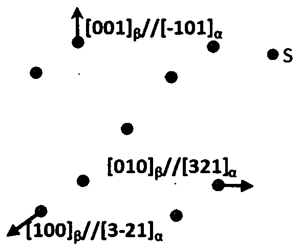
[0044] In the third step, the sample is rapidly heated until the phase changes to the BCC phase. Samples along [-101] α The direction is elongated by 1%-2%, and the shape changes.

[0045] The fourth step is to keep warm for more than 30 minutes. At this point the residual order is already at the noise level.

[0046] In the fifth step, the temperature is lowered so that the sample turns back to the monoclinic phase. At this time, the sample will no longer have the shape of the initial low-temperature phase, and the [-101] of the sample α The directions will be distributed in three equivalent directions with certain pro...


PUM

PropertyMeasurementUnit
phase transition temperatureaaaaaaaaaa

Abstract

The invention discloses a shape memory method based on order-disorder phase transition for semiconductor materials. The method realizes shape memory and shape regulation in the phase transition process by controlling the holding time of the disordered phase (high temperature phase). In the order-disorder phase transition heating and cooling phase transition cycle, single crystal Ag 2 In the order-disorder phase transition from low-temperature monoclinic phase to high-temperature body-centered cubic phase, S can memorize the shortest axis of the monoclinic phase during rapid heating and cooling cycles to realize the shape memory of the monoclinic phase. By prolonging the holding time of the high-temperature phase, the quasi-regulation of the shortest axis position and then the quasi-regulation of the shape can be realized. The invention provides a feasible idea for realizing the shape memory of semiconductors undergoing order-disorder phase transition.

Description

technical field [0001] The invention belongs to the intersection field of shape memory effect and semiconductor, and relates to a shape memory semiconductor with order-disorder phase transition and a method for realizing its shape memory and shape control. Background technique [0002] In the Ag-S binary system, only Ag 2 S a compound. Between room temperature and melting point 842°C, Ag 2 S has three isomers: monoclinic α-Ag 2 S, body centered cubic phase β-Ag 2 S and face centered cubic phase γ-Ag 2 S. where α-Ag 2 S and β-Ag 2 The equilibrium phase transition point between S is 177°C. α-Ag 2 S is also called spiral pyrite, which belongs to the monoclinic crystal system. in α-Ag 2 S atoms in S have a distorted BCC (Body Centered Cubic) structure, and the plane formed by S atoms is perpendicular to the b-axis. in α-Ag 2 There are two types of Ag atoms in S, Ag I Occupying a position slightly off the plane, the Ag II Occupies between two planes. β-Ag 2 S is ...

Claims


Application Information

Patent Timeline
Patent Type & Authority Patents(China)
IPC IPC(8): C01G5/00H01L45/00
CPCC01G5/00C01P2004/16C01P2004/04C01P2004/20H10N70/231H10N70/8822
Inventor 王勇刘军陈陆杨杭生张泽
Owner ZHEJIANG UNIV
Why Eureka
Try Eureka