

Three-dimensional memory and its manufacturing method
A manufacturing method and memory technology, which are applied to semiconductor devices, electrical solid-state devices, electrical components, etc., can solve the problems of complex circuit design and layout, and achieve the effects of avoiding connection reliability problems, simple layout, and avoiding deformation.
- Summary
- Abstract
- Description
- Claims
- Application Information
AI Technical Summary
Problems solved by technology
Method used
Image

Examples
no. 1 example
[0059] In a first exemplary embodiment of the present disclosure, a three-dimensional memory is provided.
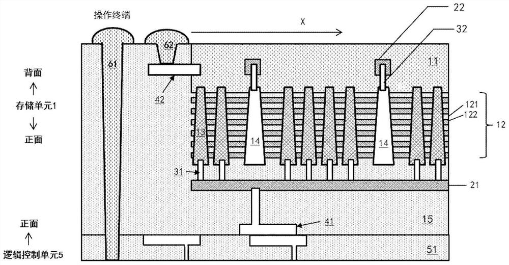
[0060] figure 2 It is a schematic cross-sectional view of the three-dimensional memory according to the first embodiment of the present disclosure.
[0061] refer to figure 2 As shown, the three-dimensional memory of the present disclosure includes: a storage unit 1 and a logic control unit 5 that are bonded to each other on the front side, and the logic control unit 5 is connected to the control circuit. It is characterized in that the second metal wire 22 of the storage unit 1 The first metal line 21 and the first metal line 21 are respectively arranged on the upper and lower sides of the channel layer 12 in the memory cell 1 , and both the first metal line 21 and the second metal line 22 are electrically connected to the control circuit.
[0062] Figure 2-Figure 3 Among them, the first metal wire 21 and the second metal wire 22 are directly or indirectly led out...
no. 2 example
[0075] In a second exemplary embodiment of the present disclosure, a three-dimensional memory is provided.
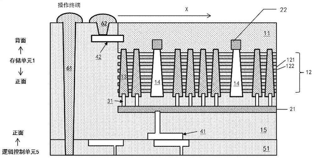
[0076] image 3 It is a schematic cross-sectional view of a three-dimensional memory according to a second embodiment of the present disclosure. Components in this embodiment that are the same as those in the first embodiment are denoted by the same reference numerals.
[0077] refer to image 3 As shown, the difference between the three-dimensional memory of this embodiment and the three-dimensional memory of the first embodiment is that the bottom of the common selection line 14 in the three-dimensional memory of this embodiment is directly electrically connected to the second metal line 22, The second connection hole 32 in the first embodiment does not exist.
no. 3 example
[0079] In a third exemplary embodiment of the present disclosure, a method for fabricating a three-dimensional memory is provided.
[0080] Figure 4 It is a flowchart of a manufacturing method for manufacturing the three-dimensional memory shown in the first embodiment according to the third embodiment of the present disclosure.
[0081] refer to Figure 4 As shown, the manufacturing method of the three-dimensional memory of the present disclosure includes:
[0082] Step S31: arranging the second metal line and the first metal line respectively on the upper and lower sides of the channel layer in the memory cell;
[0083] In this embodiment, step S31 includes:
[0084] Sub-step S31a: preparing a substrate 11;
[0085] Sub-step S31b: arranging a second metal wire 22 in the substrate 11 and insulating it from the substrate 11;
[0086] Sub-step S31c: Continue to epitaxially grow the substrate material on the substrate 11 on which the second metal line 22 has been laid, and...
PUM
 Abstract
Description
Claims
Application Information