Method for making lead frames for integrated circuit packages
A technology of lead frame and forming lead, which is applied in the direction of circuit, semiconductor/solid-state device manufacturing, electrical components, etc., and can solve the problems of long delivery time and waste of conductive layer manufacturing process
- Summary
- Abstract
- Description
- Claims
- Application Information
AI Technical Summary
Problems solved by technology
Method used
Image

Examples
Embodiment Construction
[0014] Throughout the drawings, like reference numerals refer to like elements, and the various features are not necessarily drawn to scale. In this specification, the term "couples or couples" includes indirect or direct electrical or mechanical connections or combinations thereof. For example, if a first device is coupled to or with a second device, the connection may be through a direct electrical connection, or through an indirect electrical connection through one or more intervening devices and connections.
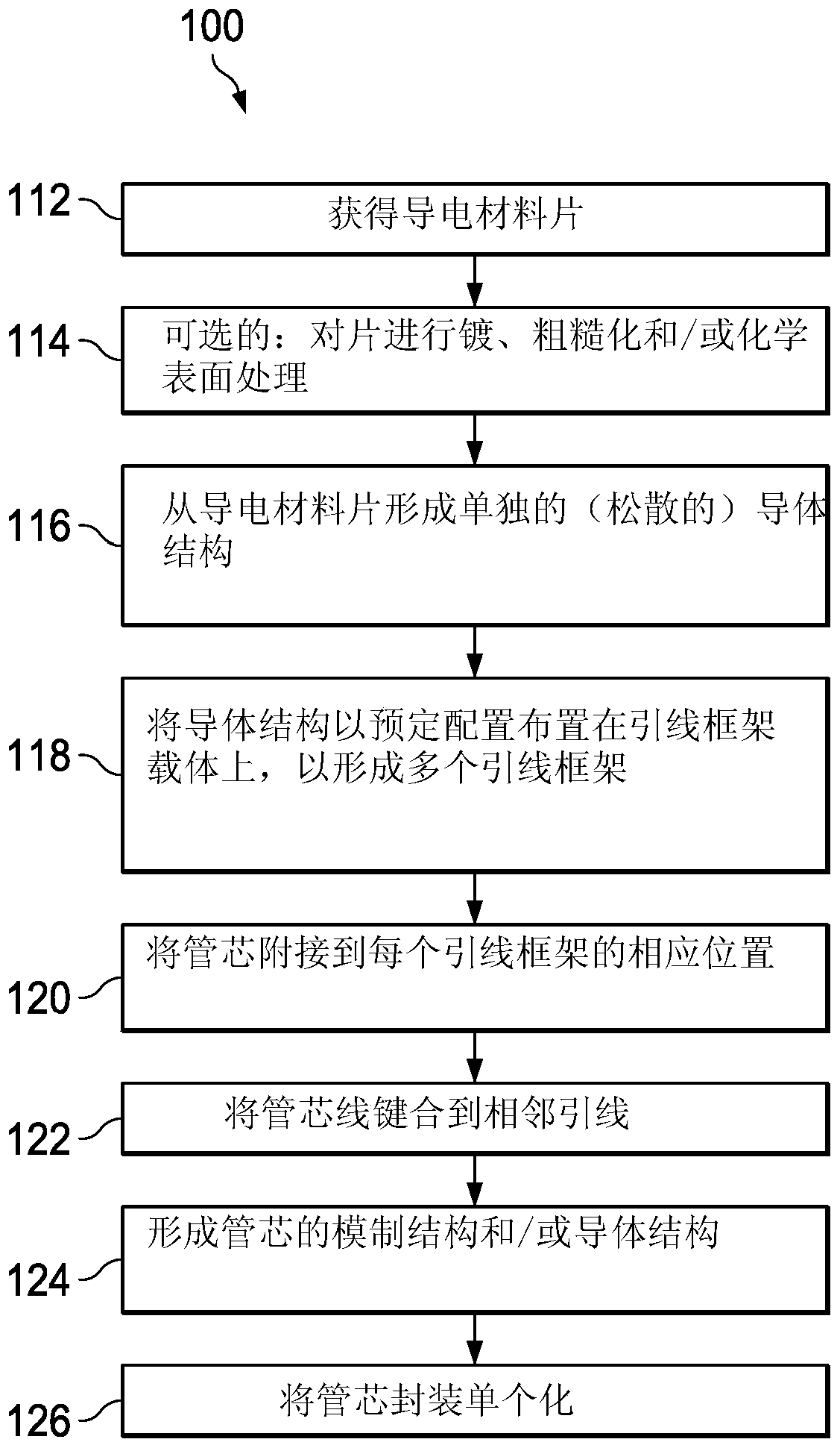
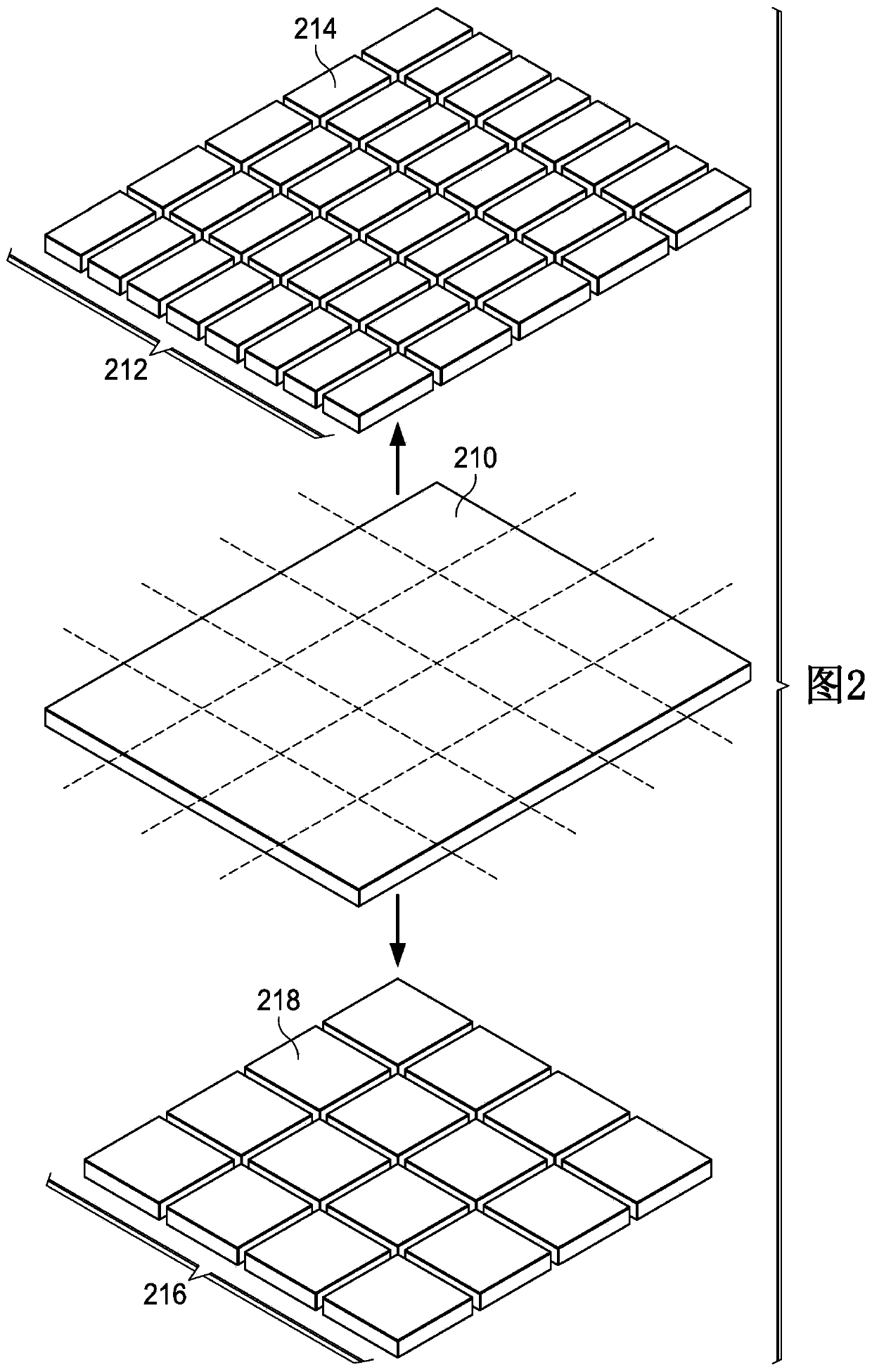
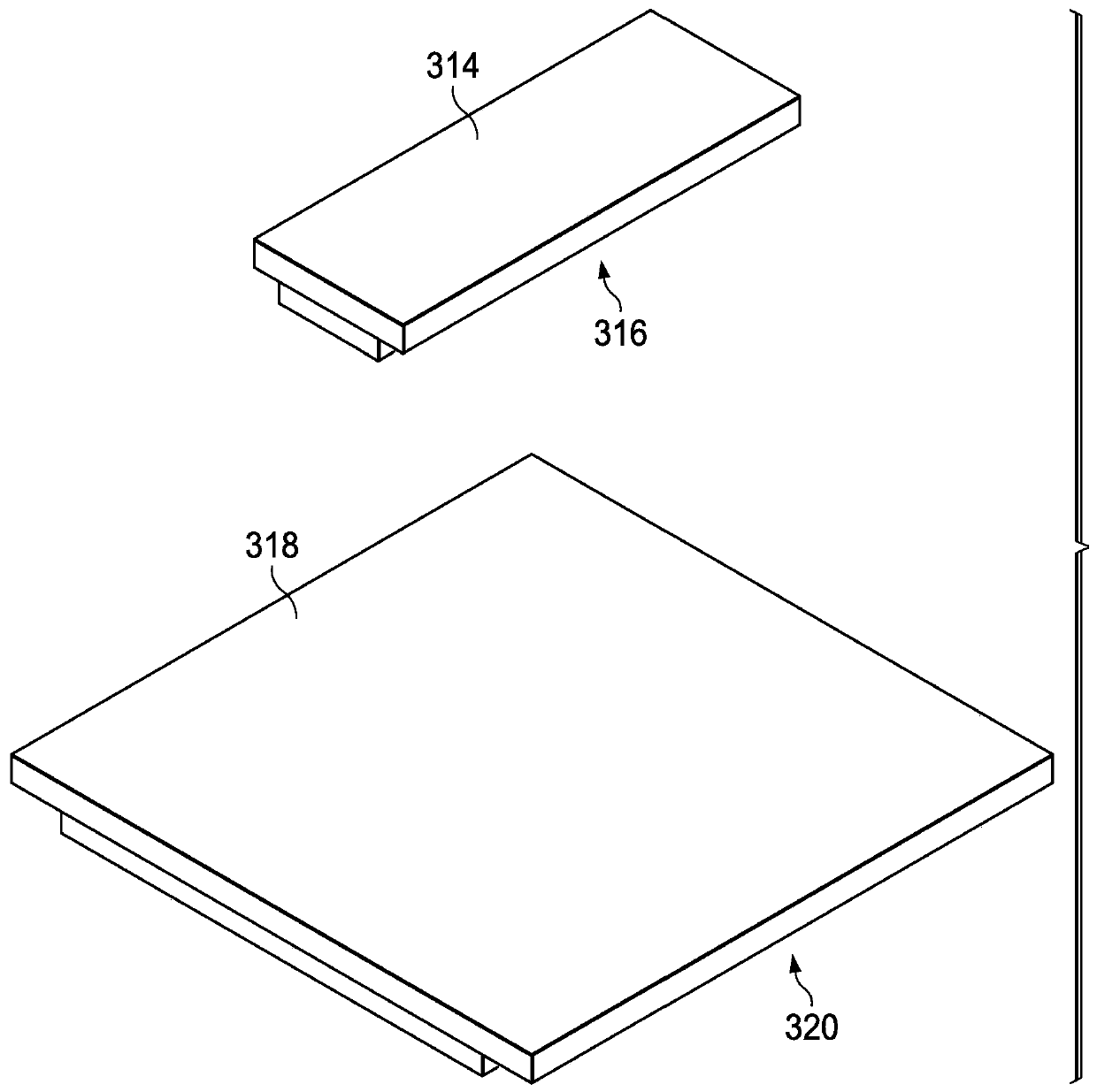
[0015] Example embodiments include methods of making leadframes that use nearly all conductor materials (incoming raw materials for leadframe conductor structures) and produce leadframes having spaced-apart conductor structures (and / or other types of structures), The spacing is less than one conductive layer thickness. This method enables the rapid generation of new leadframe configurations without redesign and can reduce the manufacturer's lead time. In one embodi...
PUM
 Abstract
Description
Claims
Application Information