Preparation method of pixel defining layer, display panel and preparation method thereof
A technology of pixel definition layer and display panel, applied in semiconductor/solid-state device manufacturing, semiconductor devices, electrical components, etc., can solve the problems affecting the life of display panel, etc., and achieve the effect of improving reliability and reducing the degree of damage
- Summary
- Abstract
- Description
- Claims
- Application Information
AI Technical Summary
Problems solved by technology
Method used
Image


Examples
Embodiment Construction
[0024] The following will clearly and completely describe the technical solutions in the embodiments of the present invention with reference to the accompanying drawings in the embodiments of the present invention. Obviously, the described embodiments are only some of the embodiments of the present invention, not all of them. Based on the embodiments of the present invention, all other embodiments obtained by persons of ordinary skill in the art without making creative efforts belong to the protection scope of the present invention.
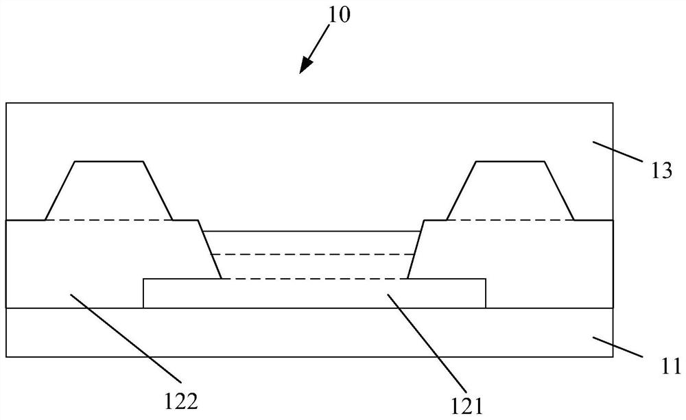
[0025] figure 1 Shown is a schematic structural diagram of a display panel in the prior art. Such as figure 1 As shown, the display panel 10 includes a substrate 11 , an organic light emitting diode structure unit layer and a thin film encapsulation layer 13 stacked in sequence from bottom to top.
[0026] The substrate 11 includes any one of a glass substrate, a metal substrate, a quartz substrate, and an organic substrate providing support, a...
PUM
 Abstract
Description
Claims
Application Information