Optical proximity effect correction method and correction system

A technology of optical proximity effect and correction conditions, applied in optics, optomechanical equipment, microlithography exposure equipment, etc., can solve the problems of wasting engineers' time, reducing the readability of recipes, increasing the length and complexity of recipes, etc., to reduce risk, increase the pass rate, and improve the effect of product pass rate

Active Publication Date: 2019-11-15
SHANGHAI HUALI INTEGRATED CIRCUTE MFG CO LTD
View PDF2 Cites 2 Cited by
  • Summary
  • Abstract
  • Description
  • Claims
  • Application Information

AI Technical Summary

Problems solved by technology

The biggest defect of the existing technology is that it can only be repaired after the defect appears, and it cannot be repaired in advance
If this type of defect does not appear once, write a recipe to fix it, which will greatly increase the length and complexity of the recipe, reduce the readability of the recipe, and waste a lot of time for engineers

Method used


Image

  • Optical proximity effect correction method and correction system
  • Optical proximity effect correction method and correction system
  • Optical proximity effect correction method and correction system

Examples


no. 1 example

[0050] The present invention provides a first embodiment of a model-based optical proximity effect correction method, which includes the following steps:

[0051] S1, based on the model, the graphic simulation on the current mask plate is formed into a photoresist profile;

[0052] S2, determining the edge position error according to the relationship between the photoresist profile and the corresponding edge position of the target pattern;

[0053] S3, screening out the opposite sides that meet the preset correction conditions;

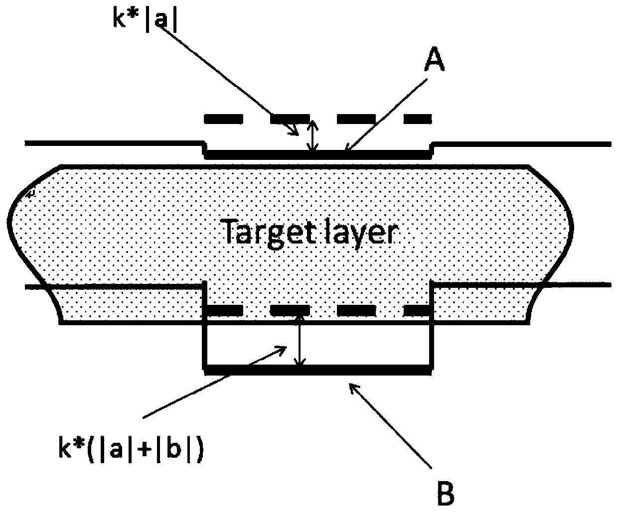
[0054] S4, calculate and screen out the pre-movement and actual movement of the opposite side;

[0055] S5, correcting the actual movement amount for the screened opposite sides respectively;

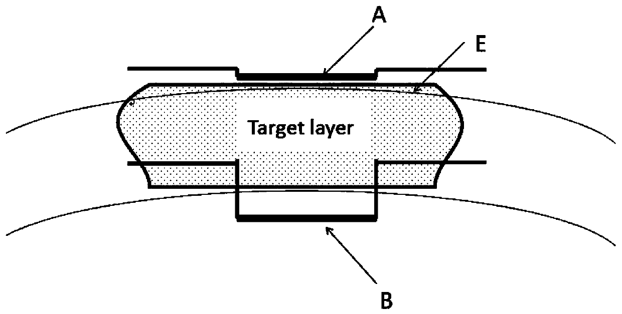
[0056] S6, repeating the above steps S2-S5 until there is no opposite edge satisfying the preset correction condition in the layout.

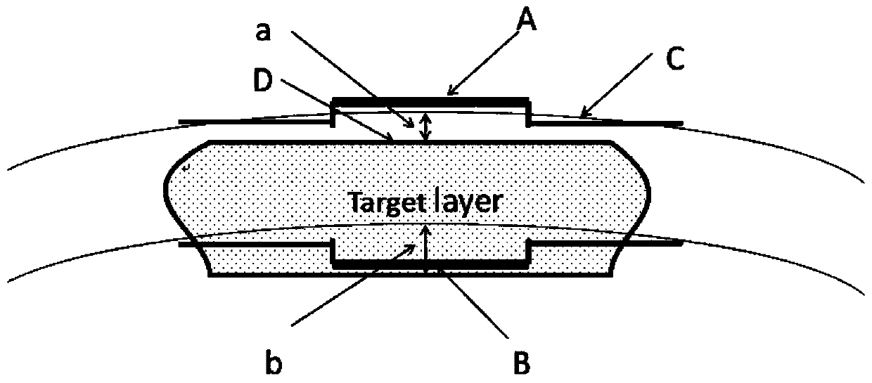
[0057] continue to combine Figure 1-Figure 3 As shown, the first embodiment of the method for correcting the proximity ef...

no. 2 example

[0060] The present invention provides a second embodiment of a model-based optical proximity effect correction method, which includes the following steps:

[0061] S1, based on the model, the graphic simulation on the current mask plate is formed into a photoresist profile;

[0062] S2. Determine the edge position error according to the positional relationship between the photoresist profile and the corresponding edge of the target pattern; determine the edge position error of the photoresist profile inside the target pattern as negative, and judge the edge position error of the photoresist profile outside the target pattern is positive; wherein, the edge position error is equal to the distance between the target pattern and the photoresist profile;

[0063] S3, screening out opposite sides whose edge position errors in the graph to be corrected are positive and negative respectively;

[0064] S4, calculate and screen out the pre-movement and actual movement of the opposite s...


PUM


Abstract

The invention discloses a model-based optical proximity effect correction method, which includes the following steps: simulating a pattern on a current mask to form a photoresist contour based on a model; determining the edge placement error according to the position relationship between the photoresist contour and the corresponding sides of a target pattern; screening out opposite sides satisfying preset correction conditions; calculating the pre-movement amount and actual movement amount of the opposite sides; correcting the actual movement amount of the opposite sides screened out; and repeating the steps above until there are no opposite sides in the layout which satisfy the preset correction conditions. The invention also discloses a model-based optical proximity effect correction system. The optical proximity effect correction method / correction system of the invention can reduce the risk of product defects and improve the qualification rate of products by properly increasing theamount of movement of one of opposite sides about to move in the same direction in the future in advance during same-order iteration of optical proximity effect correction.

Description

technical field [0001] The invention relates to the field of semiconductors, in particular to a model-based optical proximity effect correction method. The invention also relates to a model-based optical proximity effect correction system. Background technique [0002] Optical proximity correction (OPC) is a lithography enhancement technology. Optical proximity correction (OPC) is mainly used in the production process of semiconductor chips to ensure that the edges of the graphics designed in the production process are completely etched. Irregularities in these projected images, such as narrower or wider line widths than designed, can be compensated for by changing the reticle. Other distortions, such as rounded corners, are limited by the resolution of the optical tool and are more difficult to compensate. These distortions, if not corrected, can significantly alter the electrical performance of the produced circuit. Optical proximity correction corrects these errors by ...

Claims


Application Information

Patent Timeline
Patent Type & Authority Applications(China)
IPC IPC(8): G03F7/20G03F1/36
CPCG03F1/36G03F7/70441
Inventor 乔彦辉王丹于世瑞
Owner SHANGHAI HUALI INTEGRATED CIRCUTE MFG CO LTD
Why Eureka
Try Eureka