Method of manufacturing capacitor assembly and semiconductor stacked packaging method

A technology for capacitor components and manufacturing methods, which is applied in semiconductor devices, semiconductor/solid-state device manufacturing, semiconductor/solid-state device components and other directions, can solve problems such as size reduction and package warpage, and achieve size reduction and flexibility. The effect of performance and simple preparation process

Inactive Publication Date: 2019-11-15
南通沃特光电科技有限公司
4 Cites 1 Cited by

AI-Extracted Technical Summary

Problems solved by technology

For some integrated circuit packages with specific functions, it is often necessary to integrate capacitor devices. In the prior art, capacitors are often combined and packaged as an independent chip, or an embedded capacitor str...

Abstract

The invention provides a method of manufacturing a capacitor assembly and a semiconductor stacked packaging method. A separate capacitor assembly module is used for integrated packaging, the packagingsize can be reduced, the packaging flexibility is improved at the same time, and the cost is reduced. The capacitor assembly comprises a capacitor structure and a through-hole structure. The manufacturing process is simple, two structures can be formed by using a conductive layer, etching depths are different, and electrical connection positions of upper through-holes are caused to be different.

Application Domain

Semiconductor/solid-state device detailsSolid-state devices +2

Technology Topic

CapacitanceElectricity +3

Image

  • Method of manufacturing capacitor assembly and semiconductor stacked packaging method
  • Method of manufacturing capacitor assembly and semiconductor stacked packaging method
  • Method of manufacturing capacitor assembly and semiconductor stacked packaging method

Examples

  • Experimental program(1)

Example Embodiment

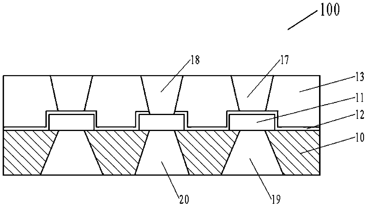
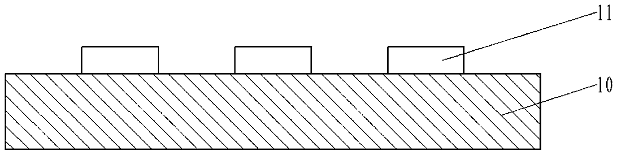
[0026] see figure 1 , the present invention provides a capacitor assembly 100 , the capacitor assembly 100 includes a substrate 10 and a capacitor structure and a through hole structure on the substrate 10 . The capacitor structure includes a first upper through hole 17 , a dielectric layer 12 , a conductive layer 11 and a first lower through hole 19 , the through hole structure includes a second upper through hole 18 , a conductive layer 11 and a second lower through hole 20 , Wherein, the first and second lower through holes 19 and 20 are disposed in the substrate 10 and formed in the same steps by the same process. The conductive layer 11 is deposited on the substrate 10 and has a plurality of discrete conductive patterns corresponding to and physically connected to the first and second lower vias 19 and 20, respectively. The dielectric layer 12 covers the substrate 10 and the conductive layer 11 , and only has an opening at the bottom of the second upper via 18 , which exposes the conductive layer 11 . A low-K material layer 13 is formed on the dielectric layer 12 , and the first and second upper vias 17 and 18 are formed on the low-K material layer 13 . The bottom of the first upper via 17 is physically In contact with the dielectric layer 12 , the bottom of the second upper through hole 18 is in physical contact with the conductive layer 11 . The first upper through hole 17 serves as the upper plate of the capacitor structure, and the first lower through hole 19 and the conductive layer 12 serve as the lower plate of the capacitor structure.
[0027] For the manufacturing method of the above capacitor structure, see Figure 3-8 , see first image 3 , depositing a patterned conductive layer 11 on the substrate 10, wherein the substrate 10 is a silicon substrate, and the conductive layer 11 is any one of aluminum, copper, titanium, titanium nitride, tantalum, and tantalum nitride one or more combinations.
[0028] see Figure 4 , covering the substrate 10 and the conductive layer 11 with a dielectric layer 12, the dielectric layer 12 is a high-K material, such as ZrO 2 , Al 2 O 3 , Si 3 N 4 , HfO 2 , Y 2 O 3 , SiO 2 , Ta 2 O 5 , La 2 O 3 , TiO 2.
[0029] see Figure 5 , forming a low-K material layer 13 on the dielectric layer 12, and forming a first opening 14 and a second opening 15 in the low-K material layer 13 through the first etching, wherein the first opening 14 and the second openings 15 correspond to the patterned conductive layer 11 , and the bottoms of the first openings 14 and the second openings 15 expose the dielectric layer 12 . Wherein, the low-K material layer 13 is silicon oxide or silicon nitride.
[0030] see Image 6 and performing a second etching on the second opening 15 therein to etch away the dielectric layer at the bottom of the second opening 15 to form a third opening 16 , wherein the third opening 16 exposes the conductive layer 11 .
[0031] see Figure 7 , filling the first opening 14 and the third opening 16 with a conductive substance to form a first upper through hole 17 and a second upper through hole 18 , wherein the first upper through hole 17 and the conductive layer 11 pass through The dielectric layers 11 are separated, and the second upper through holes 18 are electrically connected to the conductive layers 11 .
[0032] see Figure 8 , opening from the back of the substrate 10 to form a fourth opening and a fifth opening, and filling the fourth opening and the fifth opening with a conductive substance to form a first lower through hole 19 and a second lower through hole 20 , wherein the first lower through-hole 19 corresponds to the first upper through-hole 17 one-to-one, the second lower through-hole 20 corresponds to the second upper through-hole 18 one-to-one, and the first and the second lower through holes are electrically connected to the conductive layer 11 .
[0033] In integrated circuit packaging, the capacitor assembly is package-friendly. For details, see figure 2 , the package body includes a first redistribution layer 28 having a first surface and a second surface, a first chip 22 and at least one of the above-mentioned capacitor components 100 are arranged on the first redistribution layer 28, the first redistribution layer 28 The chip 22 and the first and second lower vias 19 , 20 of the capacitor assembly 100 are electrically connected to the first redistribution layer 28 . The first plastic encapsulation layer 23 seals the first chip 22 and the capacitor element 100 , the top surface of the capacitor element 100 is flush with the top surface of the first plastic encapsulation layer 23 , and the first and second tops are connected to each other. The holes 17 and 18 are exposed from the top of the first plastic sealing layer 23 . The second redistribution layer 24 is formed on the first plastic sealing layer 23 , and the first and second upper through holes 17 and 18 are electrically connected to the second redistribution layer 24 . The second chip 25 is electrically connected on the second redistribution layer 24 through solder balls 26 , and the second chip 25 is sealed by a second plastic sealing layer 27 . In addition, the second surface also has external connection terminals 29 , such as solder balls, etc., which are electrically connected to the first redistribution layer 28 .
[0034] For the manufacturing method of the above-mentioned package structure, see Figure 9-13 , see first Figure 9 , the first chip 22 and a plurality of capacitor components 100 are fixedly placed on the temporary carrier 21 , wherein the capacitor components 100 are arranged around the first chip 22 .
[0035] see Figure 10 , the first chip 22 and the plurality of capacitor components 100 are sealed by the first plastic sealing layer 23 , wherein the top surface of the capacitor components 100 is flush with the top surface of the first plastic sealing layer 23 , and the first The first and second upper through holes 17 and 18 are exposed from the top of the first plastic sealing layer 23 .
[0036] see Figure 11 , a second redistribution layer 24 is formed on the first plastic sealing layer 23 , and the first and second upper through holes 17 and 18 are electrically connected to the second redistribution layer 24 . The second chip 25 is electrically connected on the second redistribution layer 24 through solder balls 26 , and the second chip 25 is sealed by a second plastic sealing layer 27 .
[0037] see Figure 12 , and peel off the temporary carrier 21 .
[0038] see Figure 13 , a first redistribution layer 28 is formed under the first plastic packaging layer 23, and the first chip 22 and the first and second lower through holes 19, 20 of the capacitor assembly 100 are electrically connected to the first Redistribution layer 28 . Finally, external connection terminals 29 are formed under the first redistribution layer 28 .
[0039] Finally, it should be noted that: obviously, the above-mentioned embodiments are only examples for clearly illustrating the present invention, and are not intended to limit the implementation manner. For those of ordinary skill in the art, changes or modifications in other different forms can also be made on the basis of the above description. There is no need and cannot be exhaustive of all implementations here. However, the obvious changes or changes derived from this are still within the protection scope of the present invention.

PUM

no PUM

Description & Claims & Application Information

We can also present the details of the Description, Claims and Application information to help users get a comprehensive understanding of the technical details of the patent, such as background art, summary of invention, brief description of drawings, description of embodiments, and other original content. On the other hand, users can also determine the specific scope of protection of the technology through the list of claims; as well as understand the changes in the life cycle of the technology with the presentation of the patent timeline. Login to view more.

Similar technology patents

Polyaxial bone anchoring device

ActiveUS20130123861A1small sizewide application
Owner:BIEDERMANN TECH GMBH & CO KG

Handheld System for Radar Detection

InactiveUS20080169960A1high reliabilitysmall size
Owner:ROSENBURY ERWIN T

Stream encoder and stream decoder

InactiveUS20070297509A1small sizecost reduction
Owner:PANASONIC CORP

Rotary joint structure of underwater electric manipulator

InactiveCN101045301Acompact structuresmall size
Owner:SHENYANG INST OF AUTOMATION - CHINESE ACAD OF SCI

Classification and recommendation of technical efficacy words

  • small size
  • increase flexibility

Microfabricated elastomeric valve and pump systems

InactiveUS6929030B2high speedsmall size
Owner:CALIFORNIA INST OF TECH

RFID antenna

InactiveUS20060208900A1high efficiencysmall size
Owner:TRANSPACIFIC TECH

Capacitor module, power converter, vehicle-mounted electrical-mechanical system

ActiveUS20070109715A1reduce surge voltagesmall size
Owner:HITACHI ASTEMO LTD

Projection display chip

InactiveUS20100321640A1small sizehigh efficiency
Owner:IND TECH RES INST

Phase-change energy-storage material nanocapsule and preparation method thereof

ActiveCN104449590Asmall sizeImprove stability
Owner:INST OF CHEM MATERIAL CHINA ACADEMY OF ENG PHYSICS

Front illuminated back side contact thin wafer detectors

InactiveUS7057254B2reduce radiation damage susceptibilityincrease flexibility
Owner:OSI OPTOELECTRONICS

Security guarantee method and system for Windows terminals based on auto white list

InactiveCN101650768Aincrease flexibilityImprove the range of adaptation
Owner:SHENZHEN Y& D ELECTRONICS CO LTD

Data processing method and system

InactiveUS20070018986A1increase flexibility
Owner:IBM CORP

Urine dispersing urinal insert device

InactiveUS6920648B1increase flexibility
Owner:SUSKI MICHAEL R +1
Why Eureka
Try Eureka