Super junction MOS (Metal Oxide Semiconductor) type power semiconductor device and preparation method thereof

A technology of power semiconductors and semiconductors, applied in the fields of semiconductor/solid-state device manufacturing, semiconductor devices, electrical components, etc., can solve problems such as charge imbalance, reduce device breakdown voltage, increase turn-off loss, etc., to solve the problem of breakdown voltage Reduced, high injection efficiency effects

Inactive Publication Date: 2019-11-15
UNIV OF ELECTRONICS SCI & TECH OF CHINA
View PDF6 Cites 6 Cited by
  • Summary
  • Abstract
  • Description
  • Claims
  • Application Information

AI Technical Summary

Problems solved by technology

[0002] figure 1 The half-cell structure of a traditional Super Junction Metal Oxide Semiconductor Field Effect Transistor (SJ-MOSFET) is shown. SJ-MOSFET is a multi-subtype device controlled by an insulated gate. There are P-type pillar regions and N-type pillar regions with opposite doping types in the region, and the charge balance effect brought by them can improve the breakdown voltage of the device. However, in the actual process, the process of etching the P-type pillar regions will It presents a certain angle, so that the groove of the etched P-type column area is trapezoidal. This trapezoidal groove will cause the charge imbalance between the P-type column area and the N-type column area, thereby reducing the breakdown voltage of the device.
In addition, due to the structural characteristics of the super-junction MOSFET and the high injection efficiency on the source side, a large number of non-equilibrium carriers will be stored in the drift region during the reverse conduction process, and a large number of non-equilibrium carriers will increase the bulk density. The reverse recovery time of the diode increases the turn-off loss, which deteriorates the reverse recovery characteristics of the body diode in the MOSFET
Therefore, there is an urgent need for a new super-junction MOS power semiconductor device to solve the problems of reduced breakdown voltage and worsened reverse recovery characteristics of the body diode caused by the charge imbalance caused by the actual process.

Method used


Image

  • Super junction MOS (Metal Oxide Semiconductor) type power semiconductor device and preparation method thereof
  • Super junction MOS (Metal Oxide Semiconductor) type power semiconductor device and preparation method thereof
  • Super junction MOS (Metal Oxide Semiconductor) type power semiconductor device and preparation method thereof

Examples


Embodiment Construction

[0051] The principles and features of the present invention are described below in conjunction with the accompanying drawings, and the examples given are only used to explain the present invention, and are not intended to limit the scope of the present invention.

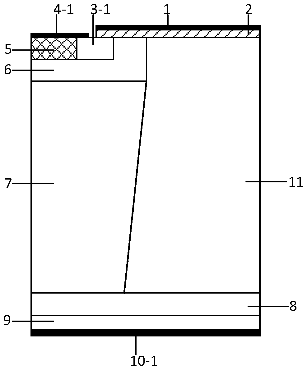
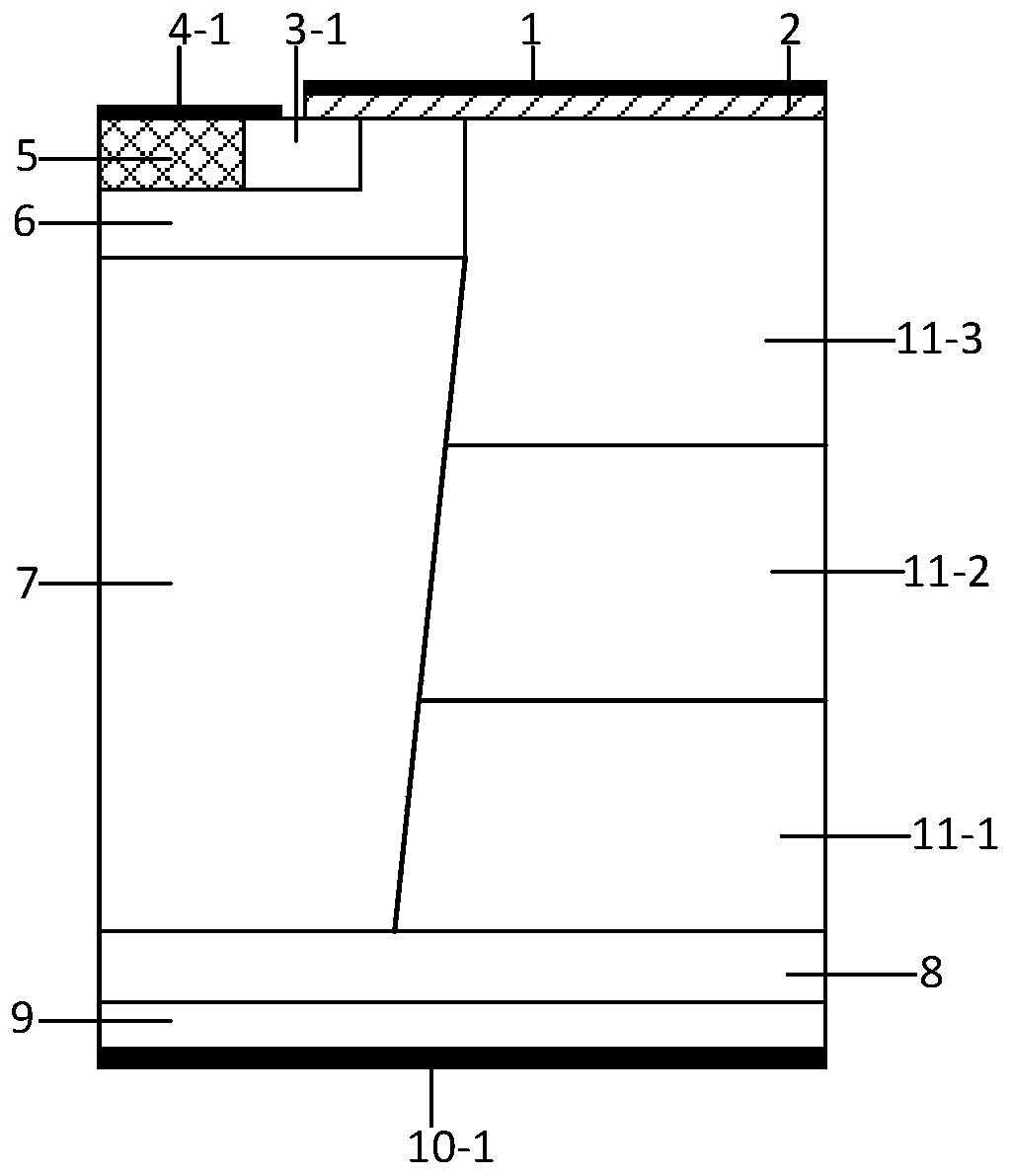
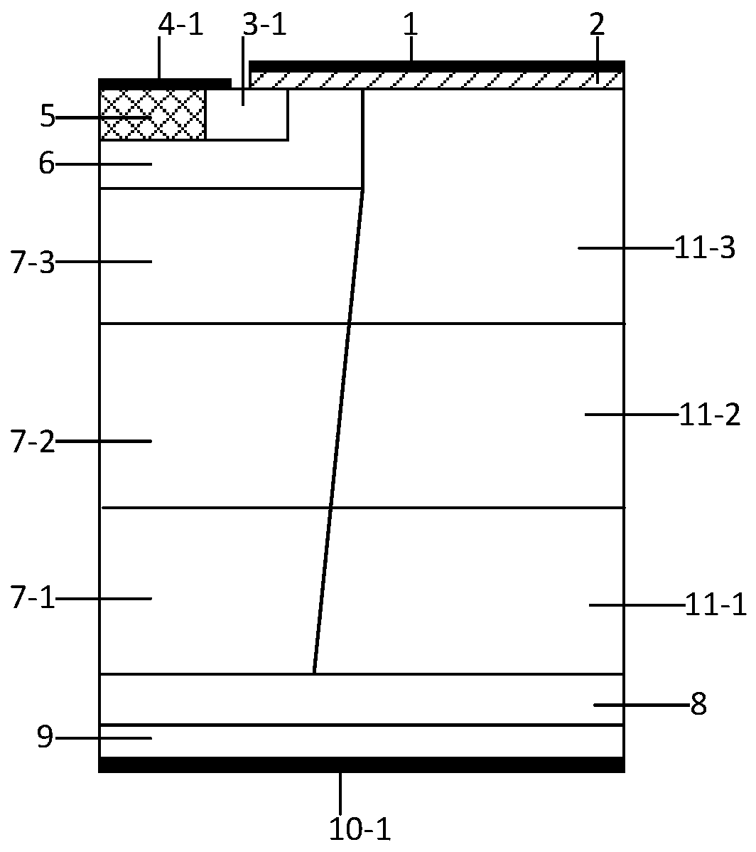
[0052] like figure 2 As shown, a super junction MOS type power semiconductor device provided by the first embodiment of the present invention includes: a metallized drain 10-1, a first conductivity type semiconductor drain region 9, a first conductivity type semiconductor field stop layer 8, The second conductivity type semiconductor column area 7, the first conductivity type semiconductor first column area 11-1, the first conductivity type semiconductor second column area 11-2, the first conductivity type semiconductor third column area 11-3, the second Conduction type semiconductor base region 6, second conductivity type semiconductor layer 5, first conductivity type semiconductor source region 3-1, planar gate s...


PUM


Abstract

The invention relates to a super junction MOS (Metal Oxide Semiconductor) type power semiconductor device and a preparation method thereof, and belongs to the technical field of power semiconductors.The invention provides a power semiconductor device which comprises a multi-layer first conduction type semiconductor column region and uses a heterojunction as an unbalanced carrier barrier, realizesa charge balance effect, reduces the high injection efficiency at one side of a source electrode, solves the problems of reduced breakdown voltage and deteriorated reverse recovery characteristic ofa body diode caused by charge imbalance brought about by the actual process, improves the breakdown voltage of the device and improves the reverse recovery characteristic of the body diode. In addition, the invention further provides a preparation method of the super junction MOS type power semiconductor device, which is simple and controllable in manufacturing process and has strong compatibilitywith the existing process.

Description

technical field [0001] The invention belongs to the technical field of power semiconductors, and in particular relates to a super-junction MOS power semiconductor device and a preparation method thereof. Background technique [0002] figure 1 The half-cell structure of a traditional Super Junction Metal Oxide Semiconductor Field Effect Transistor (SJ-MOSFET) is shown. SJ-MOSFET is a multi-subtype device controlled by an insulated gate. There are P-type pillar regions and N-type pillar regions with opposite doping types in the region, and the charge balance effect brought by them can improve the breakdown voltage of the device. However, in the actual process, the process of etching the P-type pillar regions will It presents a certain angle, so that the groove of the etched P-type column area is trapezoidal. This trapezoidal groove will cause the charge imbalance between the P-type column area and the N-type column area, thereby reducing the breakdown voltage of the device. ...

Claims


Application Information

Patent Timeline
Patent Type & Authority Applications(China)
IPC IPC(8): H01L29/06H01L29/78H01L21/336
CPCH01L29/0634H01L29/0684H01L29/66666H01L29/7827
Inventor 张金平罗君轶赵阳刘竞秀李泽宏张波
Owner UNIV OF ELECTRONICS SCI & TECH OF CHINA
Why Eureka
Try Eureka