Silicon carbide MOS device with majority carrier diode

A majority carrier, MOS device technology, applied in the field of silicon carbide MOS devices, can solve the problems of large proportion, increase the conduction loss of MOS devices, and affect the reverse breakdown voltage of MOS devices, etc.

Inactive Publication Date: 2019-11-19
PN JUNCTION SEMICON HANGZHOU CO LTD
View PDF5 Cites 2 Cited by
  • Summary
  • Abstract
  • Description
  • Claims
  • Application Information

AI Technical Summary

Problems solved by technology

First of all, the reverse leakage of the Schottky diode is large. If the area occupied by the parasitic Schottky diode is too large during device design, it will affect the reverse breakdown voltage of the MOS device.
Secondly, the voltage drop of the Schottky diode itself is too large when the current is high, which will make the voltage drop loss

Method used


Image

  • Silicon carbide MOS device with majority carrier diode
  • Silicon carbide MOS device with majority carrier diode
  • Silicon carbide MOS device with majority carrier diode

Examples


Embodiment Construction

[0013] In order to make the object, technical solution and advantages of the present invention clearer, the present invention will be described in further detail below in conjunction with the embodiments and with reference to the accompanying drawings. It should be understood that the specific embodiments described here are only used to explain the present invention, not to limit the present invention.

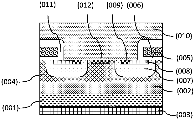
[0014] Embodiments of the present invention are as figure 1 As shown, the silicon carbide substrate (001), drift region (002), current enhancement injection region (004) and source region (008) are all N-type doped, wherein the substrate (001) and source region (008) are Heavy doping, the concentration can be greater than 1E18cm -3 , the drift region (002) is lightly doped, the concentration can be 8E15cm -3 , while the doping concentration of the current-enhancing injection region (004) is higher than that of the drift region, at 1E17cm -3 about. The base region (007), th...


PUM


Abstract

The invention provides a silicon carbide MOS device with a majority carrier diode. When the MOS device is turned off, the majority carrier diode is connected in parallel with a PN junction diode, andmeanwhile, on the basis of the characteristics of the low opening voltage and single-polarity current conduction of the majority carrier diode and the large breakover current and high voltage resistance of the PN junction diode, the conduction loss of the device during reverse follow current is reduced, the reverse follow current capability and breakdown voltage of the device are improved, the reverse recovery charges of the device are reduced, and the reliability and integration of the silicon carbide MOS device are improved. When the silicon carbide MOS device is turned on, in order to reduce on resistance, the conduction loss of the MOS transistor is reduced. According to the silicon carbide MOS device of the invention, a current reinforcing injection region is additionally arranged inan active region, and the problem of excessively large JFET resistance due to excessively low epitaxial doping concentration can be solved.

Description

technical field [0001] The invention belongs to the field of semiconductors, in particular to a silicon carbide MOS device with a majority carrier diode. Background technique [0002] Silicon carbide (SiC) is currently the fastest-growing wide-bandgap power semiconductor material. MOS field-effect transistor power devices made of silicon carbide materials can withstand higher voltages and faster switching speeds than Si devices. At present, when the MOS device is turned off, the parasitic body diode in the silicon carbide field effect transistor has a large turn-on voltage, which makes the conduction loss of the MOS device become higher in the freewheeling application process. Therefore, the use of integrated majority carrier diodes in SiC MOS devices can solve this problem. In the prior art, there has been a method of using a Schottky diode as a parasitic body diode to reduce the turn-on voltage, but this method also has defects. First of all, the reverse leakage of the S...

Claims


Application Information

Patent Timeline
IPC IPC(8): H01L27/07H01L29/06H01L29/16H01L29/78
CPCH01L27/0727H01L29/0684H01L29/1608H01L29/78
Inventor 黄兴陈欣璐
Owner PN JUNCTION SEMICON HANGZHOU CO LTD
Why Eureka
Try Eureka