Background correction circuit and method for offset errors of latch type comparator
A technology for correcting circuits and comparators, applied in electrical components, analog/digital conversion calibration/testing, code conversion, etc., can solve problems such as increasing circuit complexity, and achieve circuit complexity reduction, wide correction range, and large correction range Effect
- Summary
- Abstract
- Description
- Claims
- Application Information
AI Technical Summary
Problems solved by technology
Method used
Image

Examples
Embodiment 1
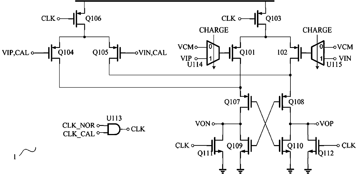
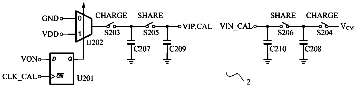
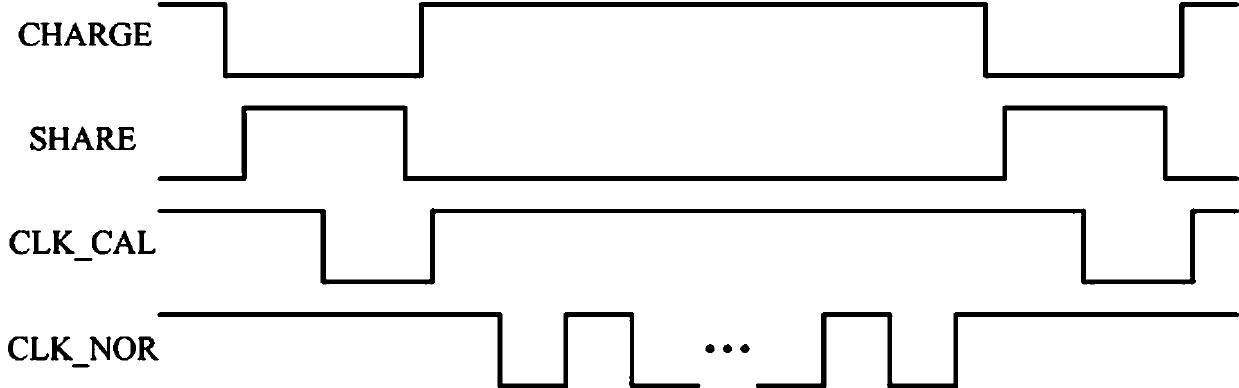
[0038] The present invention designs a background correction circuit for the offset error of the latch type comparator, without increasing the load on the output end of the latch type comparator, and only adding a pair of auxiliary input pair tubes at the drain end of the main input pair tube, such as figure 1 , figure 2 As shown, the following arrangement structure is adopted in particular: it includes a latch comparator 1 and a correction circuit 2 connected to each other, and the latch comparator 1 includes a main input pair tube, a tail current switch Q103, a load circuit, a reset circuit, In the AND gate and selector, an auxiliary input pair composed of MOS transistor Q104 and MOS transistor Q105 is provided at the drain end of the main input pair, and a tail current switch Q106 is connected to the source end of the auxiliary input pair, and the tail The current switch Q106 is commonly connected with the tail current switch Q103.
[0039] As a preferred setting scheme, ...
Embodiment 2
[0041] This embodiment is further optimized on the basis of the foregoing embodiments, and the same parts as the technical solutions of the preceding embodiments will not be repeated here, such as figure 1 , figure 2 As shown, further in order to better realize the background correction circuit of the offset error of the latch comparator described in the present invention, the following setting method is adopted in particular: the main input pair includes MOS transistors Q101 and MOS transistors Q102. The gate terminals of the MOS transistor 101 and the MOS transistor 102 are connected to a selector, the tail current switch Q103 is connected to the source terminal of the main input pair transistor, the gate terminals of the tail current switch Q103 and the tail current switch Q106 are both connected to the output terminal of the AND gate The drain end of the main input pair tube is also connected to the load circuit, the reset circuit is connected to the load circuit, and the...
Embodiment 3
[0045] This embodiment is further optimized on the basis of any of the above-mentioned embodiments, and the same parts as the technical solutions of the foregoing embodiments will not be repeated here, such as figure 1 , figure 2 As shown, further in order to better realize the background correction circuit of the offset error of the latch comparator described in the present invention, the following setting method is adopted in particular: the selector adopts a two-to-one multiplexer, and the AND The gate uses a two-input AND gate.
PUM
 Abstract
Description
Claims
Application Information
 - R&D
- Intellectual Property
- Life Sciences
- Materials
- Tech Scout
- Unparalleled Data Quality
- Higher Quality Content
- 60% Fewer Hallucinations
Browse by: Latest US Patents, China's latest patents, Technical Efficacy Thesaurus, Application Domain, Technology Topic, Popular Technical Reports.
© 2025 PatSnap. All rights reserved.Legal|Privacy policy|Modern Slavery Act Transparency Statement|Sitemap|About US| Contact US: help@patsnap.com