Organic light-emitting device taking exciplex as main body material

A technology of electroluminescent devices and host materials, which is applied in the direction of organic semiconductor devices, electric solid devices, semiconductor devices, etc., and can solve the problems of carrier recombination area concentration, carrier quenching, device efficiency and lifetime reduction, etc.

CN110492005AActive Publication Date: 2019-11-22JIANGSU SUNERA TECH CO LTD
5 Cites 26 Cited by

Patent Information

Authority / Receiving Office
CN · China
Patent Type
Applications(China)
Current Assignee / Owner
Publication Date
2019-11-22

Smart Images

  • Figure 1
    Figure 1
  • Figure 2
    Figure 2
  • Figure 3
    Figure 3
Patent Text Reader

Abstract

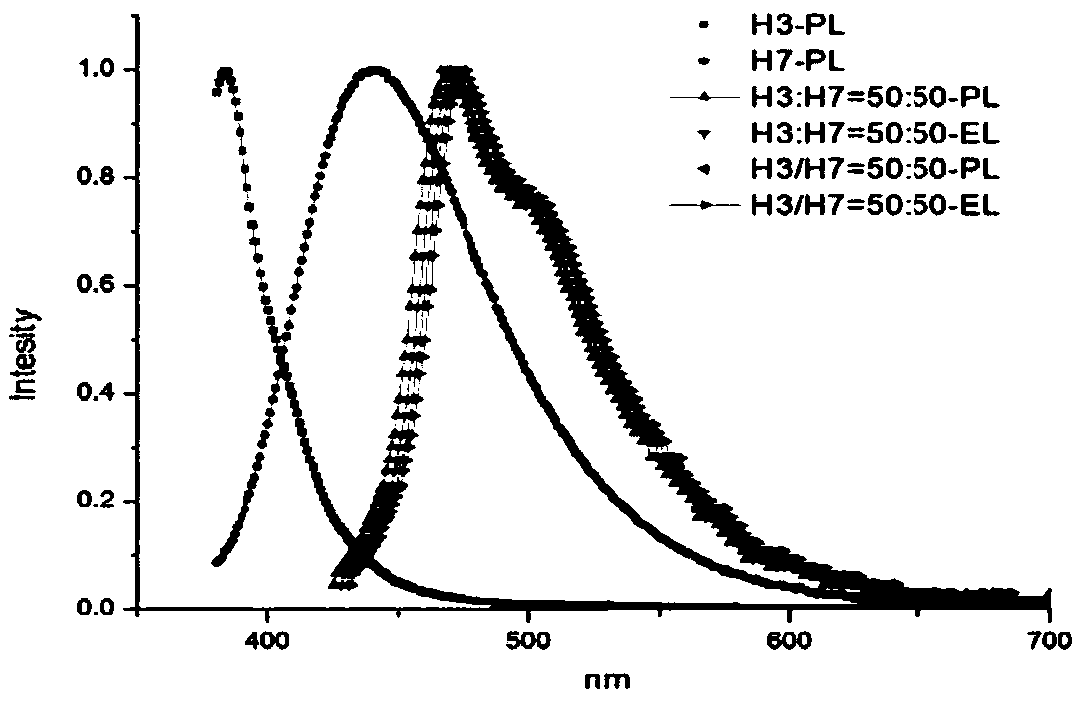
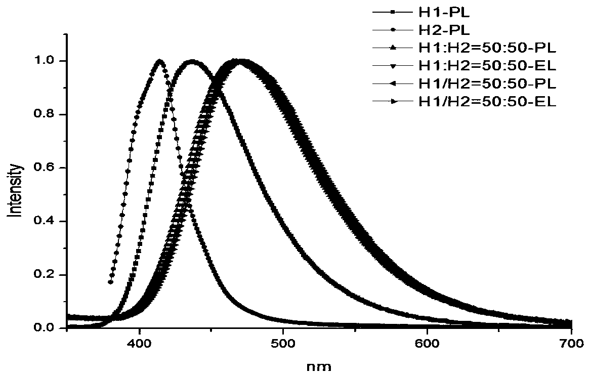
The invention relates to an organic light-emitting device taking an exciplex as a main body material, in particular to an organic light-emitting device containing the main body material and a fluorescent material, wherein the main body material comprises a first organic compound and a second organic compound, a mixture or an interface formed by the first organic compound and the second organic compound generates the exciplex under the condition of optical excitation or electric field excitation, and the emission spectrum of the formed exciplex and the absorption spectrum of the fluorescent doped material are effectively overlapped to form the effective energy transfer; the first organic compound and the second organic compound have the different carrier transport characteristics, wherein the fluorescent material is an organic compound containing the boron atoms. The organic light-emitting device prepared by the method has the characteristics of high efficiency and long service life.
Need to check novelty before this filing date? Find Prior Art

Description

technical field

[0001] The invention relates to the technical field of semiconductors, in particular to an organic electroluminescent device with high color purity, high efficiency and long life. Background technique

[0002] Organic light emitting diodes (OLEDs) have been actively researched and developed. The simplest basic structure of an organic electroluminescent device consists of a light emitting layer sandwiched between opposing cathode and anode. Organic electroluminescent devices are considered to be the next generation of flat panel displays and have attracted widespread attention because they can achieve ultra-thin and ultra-light weight, fast response to input signals, and low-voltage DC drive.

[0003] It is considered that the organic electroluminescent device has the following light emitting mechanism: when a voltage is applied between the electrodes sandwiching the light emitting layer, the electrons injected from the anode and the holes injected from the c...

Examples

Embodiment 1

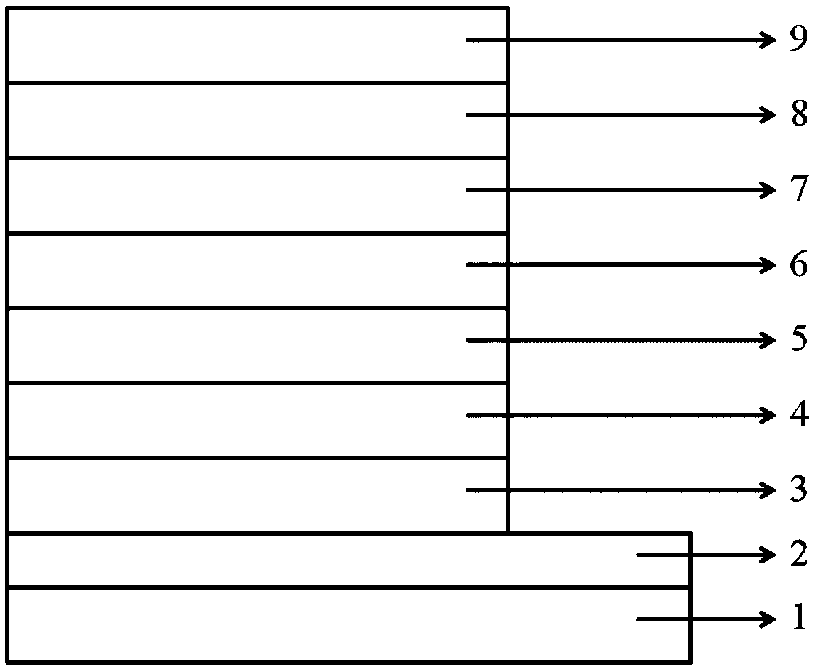
[0120] The structure of the organic electroluminescent device prepared in Example 1 is as follows: figure 1 As shown, the specific preparation process of the device is as follows:

[0121] Clean the ITO anode layer 2 on the transparent glass substrate layer 1, ultrasonically clean it with deionized water, acetone, and ethanol for 30 minutes each, and then treat it in a plasma cleaner for 2 minutes; dry the ITO glass substrate and place it in a vacuum In the cavity, the vacuum degree is less than 1*10 -6 Torr, on the ITO anode layer 2, a mixture of HT1 and P1 with a film thickness of 10 nm is evaporated, the mass ratio of HT1 and P1 is 97:3, and this layer is the hole injection layer 3; then, HT1 with a thickness of 50 nm is evaporated, and the layer As the hole transport layer 4; then vapor-deposit 20nm-thick EB1, which serves as the electron blocking layer 5; further, vapor-deposit a 25nm light-emitting layer 6, wherein the light-emitting layer includes a host material and a...

Embodiment 2~21

[0123] The preparation method is similar to that of Example 1, and the selection of specific materials is shown in Table 3.