Semiconductor structure and forming method thereof

A technology of semiconductor and gate structure, applied in the field of semiconductor structure and its formation, can solve problems such as poor performance of MOS transistors, achieve the effects of less leakage and improved performance

Active Publication Date: 2019-12-03
SEMICON MFG INT (SHANGHAI) CORP +1
View PDF22 Cites 2 Cited by
  • Summary
  • Abstract
  • Description
  • Claims
  • Application Information

AI Technical Summary

Problems solved by technology

[0003] However, with the increase in the integration of semiconductor devices, the performance of MOS transistors is poor

Method used


Image

  • Semiconductor structure and forming method thereof
  • Semiconductor structure and forming method thereof
  • Semiconductor structure and forming method thereof

Examples


Embodiment Construction

[0032] As mentioned in the background, the performance of semiconductor devices is still poor.

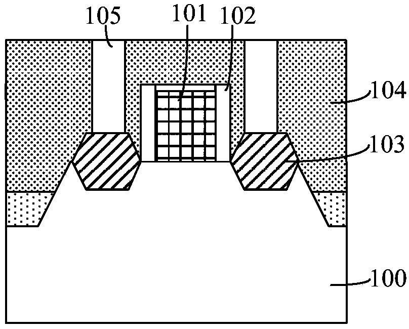
[0033] figure 1 A schematic diagram of a semiconductor structure.

[0034] Please refer to figure 1 , the substrate 100; the gate structure 101 located on the surface of the substrate 100, the sidewall of the gate structure 101 has sidewalls 102; The impurity region 103; the dielectric layer 104 located on the surface of the substrate 100 and the gate structure 101, as well as the side walls of the sidewall 102 and the source-drain doped region 103, the dielectric layer 104 has a contact hole (not shown in the figure), so The bottom of the contact hole exposes the top of the source-drain doped region 103; the plug 105 is located in the opening.

[0035] In the above semiconductor structure, the method for forming the contact hole includes: forming a mask layer on the surface of the dielectric layer 104, and the mask layer exposes the top surface of the dielectric layer 104 on th...


PUM


Abstract

The invention discloses a semiconductor structure and a forming method thereof. The forming method comprises the steps of: providing a substrate, enabling the surface of the substrate to be provided with a gate structure, and enabling the interior of the substrate at two sides of the gate structure to be provided with source-drain doped regions; forming a protective layer on part of the side wallof the gate structure; forming a first dielectric layer on the substrate, the source-drain doped region and the side wall of the protective layer; removing part of the first dielectric layer until thetop surface of the source-drain doped region is exposed, and forming a contact hole in the first dielectric layer; and forming a plug in the contact hole. The semiconductor device formed by the method is good in performance.

Description

technical field [0001] The invention relates to the field of semiconductor manufacturing, in particular to a semiconductor structure and a forming method thereof. Background technique [0002] The MOS (metal-oxide-semiconductor) transistor is an important semiconductor device. The basic structure of the MOS transistor includes: a semiconductor substrate; a gate structure located on the surface of the semiconductor substrate; a semiconductor substrate located on one side of the gate structure The source region and the drain region in the semiconductor substrate on the other side of the gate structure. [0003] However, as the integration level of semiconductor devices increases, the performance of MOS transistors is poor. Contents of the invention [0004] The technical problem solved by the invention is to provide a semiconductor structure and its forming method to improve the performance of semiconductor devices. [0005] In order to solve the above technical problems, ...

Claims


Application Information

Patent Timeline
Patent Type & Authority Applications(China)
IPC IPC(8): H01L21/336H01L29/78H01L21/8238
CPCH01L29/78H01L29/66545H01L21/823871
Inventor 周飞
Owner SEMICON MFG INT (SHANGHAI) CORP
Why Eureka
Try Eureka