Production technology for transient voltage suppressor chip with channeling effect

A technology of transient voltage suppression and channel effect, which is applied in semiconductor/solid-state device manufacturing, circuits, electrical components, etc., can solve problems such as poor uniformity of diffusion process, inaccurate control of junction depth, and influence on product reliability. Achieve the effect of good uniformity of resistivity, good consistency of electrophoresis, and easy control of junction depth

Inactive Publication Date: 2014-07-30
TIANJIN ZHONGHUAN SEMICON CO LTD
View PDF2 Cites 15 Cited by
  • Summary
  • Abstract
  • Description
  • Claims
  • Application Information

AI Technical Summary

Problems solved by technology

[0004] At present, the production process of transient voltage suppressor chips in the semiconductor industry mainly has the following problems: the paper source diffusion production process is usually used, the uniformity of the diffusion process is not good, and the junction depth control is not accurate; the existing transient voltage suppressor chips are waiting When the effective resistance is constant, the clamping voltage increases with the increase of the reverse surge current, and the increase of heat generation makes the temperature of the diffusion junction high, resulting in thermal breakdown of the device under a small reverse surge power. issues affecting product reliability

Method used


Image

  • Production technology for transient voltage suppressor chip with channeling effect
  • Production technology for transient voltage suppressor chip with channeling effect
  • Production technology for transient voltage suppressor chip with channeling effect

Examples


Embodiment Construction

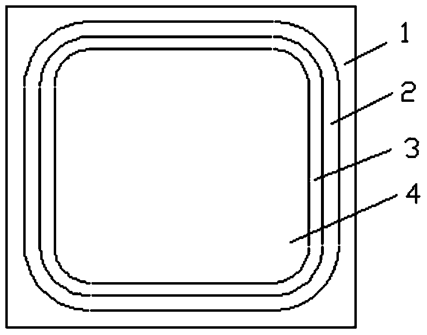
[0046] Such as figure 1 As shown, the chip structure of the transient voltage suppressor TVS is N + PN + Bi-directional high voltage transient voltage suppressor. The front section of the chip is as follows: 1TVS chip, 2 mesa grooves, 3 glass layers, 4 metal surfaces.

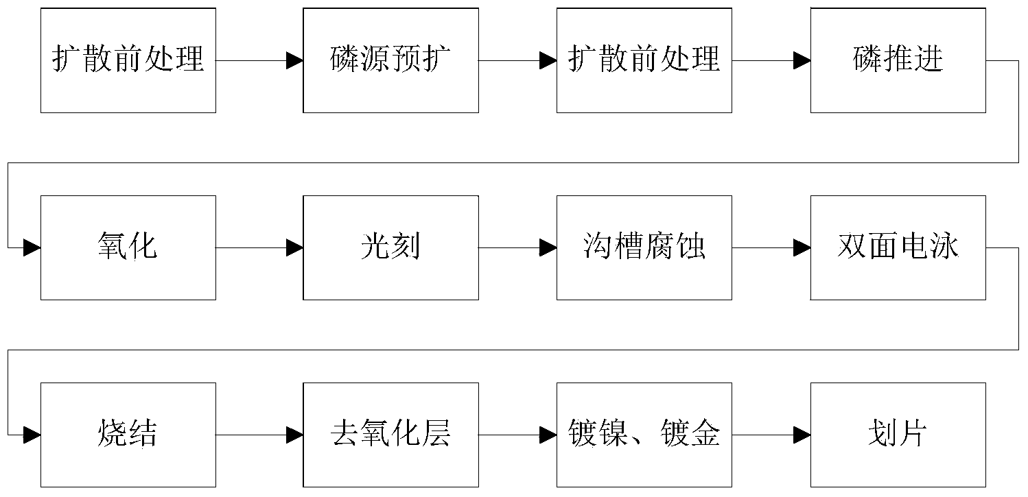
[0047] Such as figure 2 As shown, the chip process flow of the transient voltage suppressor TVS is as follows:

[0048] (1) Pre-diffusion treatment: Clean the surface of the silicon wafer through the ultrasonic cleaning process of acid, alkali and deionized water;

[0049] (2) Phosphorus source pre-expansion: Put the cleaned silicon wafer into a pre-diffusion furnace using a gaseous phosphorus source for diffusion to form a pre-expansion N + , the diffusion temperature of phosphorus source pre-expansion is 1100~1200℃, and the pre-expansion of N + Phosphorus diffusion junction sheet resistance is 0.2~0.6Ω / □, junction depth is 7~12um;

[0050] (3) Pre-diffusion treatment: acid immersion and deionized wate...


PUM


Abstract

The invention provides a production technology for a transient voltage suppressor chip with the channeling effect. By means of the steps of gaseous state source diffusion, channel corrosion and double-faced electrophoresis, in the reverse state, the width of depletion layers and the reverse voltage of the high-voltage transient voltage suppressor chip which is of the N+PN+ structure are increased along with the increase of a reverse current, when the reverse current is increased to be close to Ic, the depletion layers on the two faces make contact with each other, the channeling effect is produced, the equivalent resistance is reduced, the clamp voltage is reduced, the reverse surge capacity is improved, the reliability of a diode is improved, the service life of the diode is prolonged, and the transient voltage suppressor chip has the advantages of being good in electrical parameter uniformity, better in ohmic contact and high in reliability, the problem that the thicknesses of two glass layers are uneven due to two times of single-face electrophoresis is avoided, the glass is high in stress-resisting capability of protection and not prone to damage, and the reliability of the transient voltage suppressor chip is further improved.

Description

technical field [0001] The invention relates to the technical field of crystal diode chip production, in particular to a production process of a transient voltage suppressor chip with channel effect. Background technique [0002] The transient voltage suppressor chip (TVS) is a high-efficiency protection device in the form of a diode. When the two poles of the TVS diode are subjected to a reverse transient high-energy impact, it can turn its two poles on the order of 10-12 seconds. The high impedance between the two poles becomes low impedance, absorbing up to several thousand watts of surge power, clamping the voltage between the two poles at a predetermined value, effectively protecting the precision components in the electronic circuit from being damaged by various surge pulses. [0003] The forward characteristic of the transient voltage suppressor is the same as that of an ordinary diode, and the reverse characteristic is a typical PN junction avalanche device. Under t...

Claims


Application Information

Patent Timeline
Patent Type & Authority Applications(China)
IPC IPC(8): H01L21/329H01L21/223
CPCH01L21/223H01L29/6609
Inventor 薄勇刘长蔚白树军
Owner TIANJIN ZHONGHUAN SEMICON CO LTD
Why Eureka
Try Eureka