Printing ink printing method and capacitive type touch screen laser etching technology
A technology of ink printing and ink, which is applied in printing, printing devices, electrical digital data processing, etc., can solve the problems that ink is easily broken down by laser and the yield rate of capacitive touch screen is low, so as to achieve the effect of improving yield rate
- Summary
- Abstract
- Description
- Claims
- Application Information
AI Technical Summary
Problems solved by technology
Method used
Image

Examples
Embodiment 1
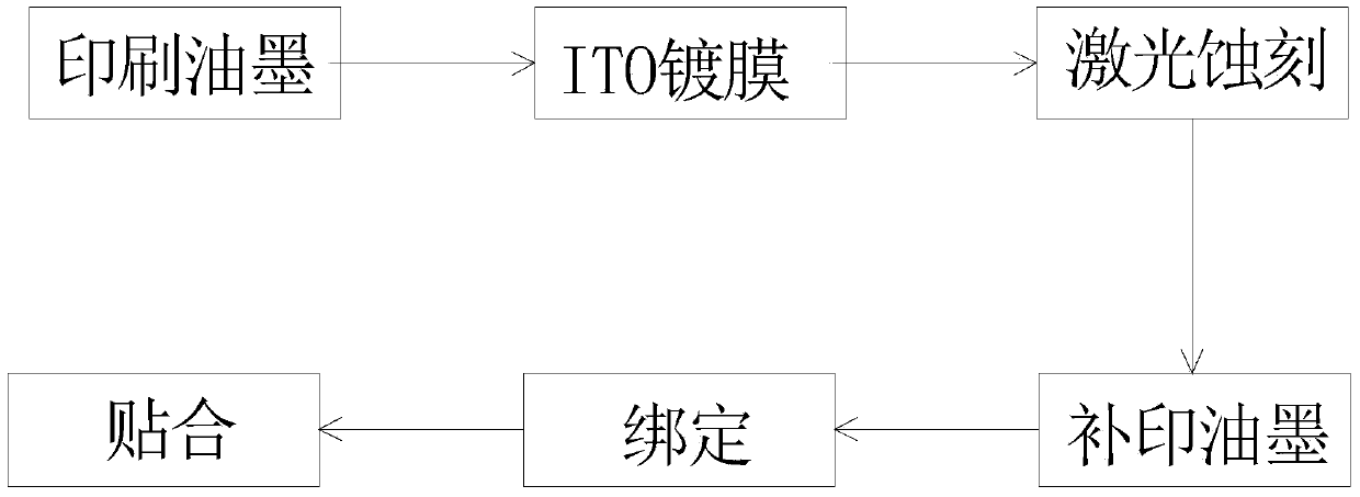
[0033] The capacitive touch screen laser etching process provided in this embodiment includes the following steps:
[0034] A: Printing ink process, which includes the following steps in sequence:
[0035] Step 1: A step of printing white ink on the cover plate, the cover plate includes a frame and a binding area located on the frame, wherein, in step 1, a layer of white ink is printed on the cover plate, and the white ink layer covers the The thickness of the white ink layer printed on the cover frame is 8 μm in the entire frame area of the binding area on the cover frame;
[0036] Step 2: a step of baking and curing the white ink layer on the cover plate;
[0037] B: ITO coating process, evenly coating a layer of ITO conductive film on the cover plate;
[0038] C: Laser etching process, using a laser with a wavelength of 532nm to etch the cover plate coated with ITO conductive film to obtain an ITO circuit;
[0039] D: Reprinting frame ink process, covering the lasered ...
Embodiment 2
[0047] The difference between this embodiment and the foregoing embodiments is only in process A, and process A is described in detail below:
[0048] A: Printing ink process, which includes the following steps in sequence:
[0049] Step 1: a step of printing white ink on the cover plate, wherein, in step 1, a layer of white ink layer is printed on the cover plate, and the white ink layer covers the entire frame area including the binding area on the frame of the cover plate, The thickness of the white ink layer printed on the frame of the cover is 16 μm;
[0050] Step 2: a step of baking and curing the white ink layer on the cover plate;
[0051] Wherein, in step 1, the white ink layer is divided into two layers of oil for printing, and the thickness of each white ink layer is 8 μm.
[0052] Wherein, in step 1, the fluid of the white ink layer is leak-printed on the cover plate through the screen by using a screen printing machine, and the mesh number of the screen printing...
Embodiment 3
[0056] The difference between this embodiment and the foregoing embodiments is only in process A, and process A is described in detail below:
[0057] A: Printing ink process, which includes the following steps in sequence:
[0058] Step A: printing a black ink layer or a colored ink layer on the frame of the cover plate;
[0059] Step B: a step of baking and curing the black ink layer or the colored ink layer on the cover plate;
[0060] Step 1: a step of printing white ink on the cover plate, wherein the white ink layer only covers the binding area of the cover plate, and the thickness of the white ink layer is 8 μm;
[0061] Step 2: a step of baking and curing the white ink layer on the cover plate;
[0062] Wherein, the thickness of the black ink layer or the color ink layer is 4 μm.
[0063] Wherein, in step B, the curing temperature of the black ink layer or the colored ink is 150°, and the curing time is 10 minutes.
[0064] Wherein, in step A, the black ink layer...
PUM
| Property | Measurement | Unit |
|---|---|---|
| thickness | aaaaa | aaaaa |
| thickness | aaaaa | aaaaa |
| thickness | aaaaa | aaaaa |
Abstract
Description
Claims
Application Information
 - R&D
- Intellectual Property
- Life Sciences
- Materials
- Tech Scout
- Unparalleled Data Quality
- Higher Quality Content
- 60% Fewer Hallucinations
Browse by: Latest US Patents, China's latest patents, Technical Efficacy Thesaurus, Application Domain, Technology Topic, Popular Technical Reports.
© 2025 PatSnap. All rights reserved.Legal|Privacy policy|Modern Slavery Act Transparency Statement|Sitemap|About US| Contact US: help@patsnap.com