Laminated complementary metal oxide semiconductor image sensor and image processing method

An oxide semiconductor and image sensor technology, applied in the field of image processing, can solve the problems of large thickness, high power consumption and large pixel size of complementary metal oxide semiconductor image sensors

Inactive Publication Date: 2019-12-03
GUANGDONG OPPO MOBILE TELECOMM CORP LTD
View PDF11 Cites 10 Cited by
  • Summary
  • Abstract
  • Description
  • Claims
  • Application Information

AI Technical Summary

Problems solved by technology

[0003] However, the existing three-layer photosensitive element has problems of large pixel size and high power consumption of CMOS image sensors due to the large thickness of each layer of photosensitive element.

Method used


Image

  • Laminated complementary metal oxide semiconductor image sensor and image processing method
  • Laminated complementary metal oxide semiconductor image sensor and image processing method
  • Laminated complementary metal oxide semiconductor image sensor and image processing method

Examples


Embodiment 1

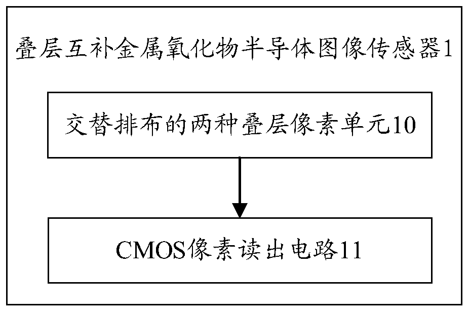
[0049] An embodiment of the present application provides a stacked complementary metal oxide semiconductor image sensor 1, such as figure 1 As shown, the stacked complementary metal oxide semiconductor image sensor 1 includes:

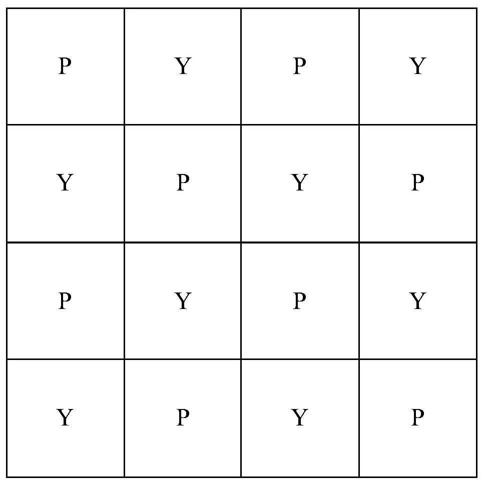
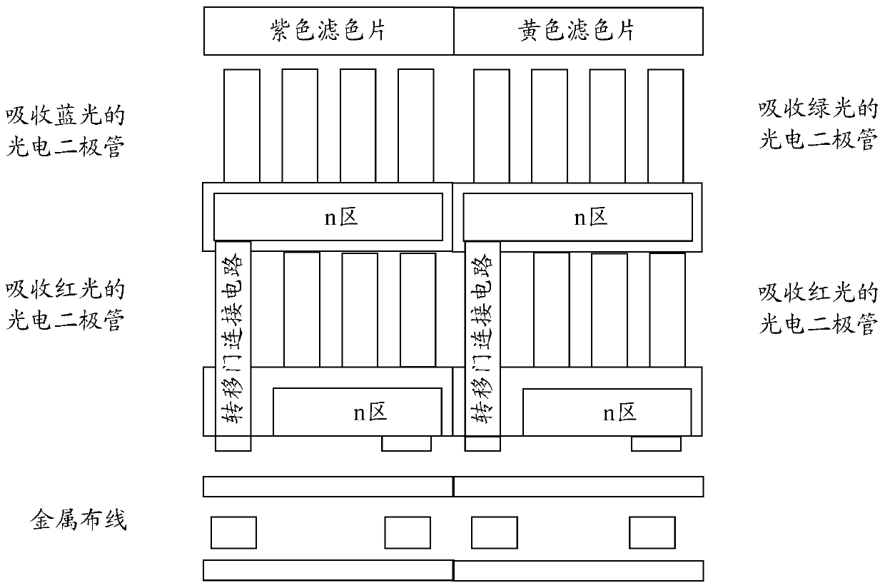
[0050] Two kinds of stacked pixel units 10 arranged alternately, the two kinds of stacked pixel units 10 include photodiode PD columns 100 of three sizes, wherein each of the two kinds of stacked pixel units 10 is stacked The pixel units are respectively arranged with two layers of PD columns 100. The two layers of photodiode PD columns 100 include PD columns of two sizes, and the size of each layer of PD columns in the two layers of PD columns 100 is the same. The layer pixel unit 10 uses the PD columns of the three sizes to absorb the RGB three-color lights respectively, and converts the optical signals corresponding to the RGB three-color lights into electrical signals corresponding to the RGB three-color lights;

[0051] A CMOS pixel readout circu...

Embodiment 2

[0103] An embodiment of the present application provides an image processing method, which is applied to a stacked complementary metal oxide semiconductor image sensor. The stacked complementary metal oxide semiconductor image sensor includes two types of stacked pixel units and CMOS pixel readout circuits arranged alternately. The two types of stacked pixel units include three sizes of PD columns, wherein each of the two types of stacked pixel units includes PD columns of two sizes, such as Image 6 As shown, the method may include:

[0104] S101. Utilize two sizes of PD columns of each stacked pixel unit to absorb two kinds of RGB monochromatic lights sequentially, so as to use three sizes of PD columns to respectively absorb RGB three-color lights, and convert the optical signals corresponding to the RGB three-color lights into an electrical signal.

[0105] An image processing method provided in an embodiment of the present application is applicable to a scenario where im...

Embodiment 3

[0124] An embodiment of the present application provides a storage medium on which a computer program is stored. The computer-readable storage medium stores one or more programs, and the one or more programs can be executed by one or more processors. In the CMOS image sensor 1, the computer program realizes the image processing method as described in the second embodiment.

[0125] Specifically, when the program instructions corresponding to an image processing method in this embodiment are read or executed by an electronic device, the following steps are included:

[0126] The two sizes of PD columns of each stacked pixel unit are used to absorb two kinds of RGB monochromatic lights in sequence, so that the three sizes of PD columns are used to absorb RGB three-color lights respectively, and the RGB three-color lights correspond to The optical signal is converted into an electrical signal;

[0127] The electrical signal is amplified by the CMOS pixel readout circuit, and the...


PUM


Abstract

The embodiment of the invention provides a laminated complementary metal oxide semiconductor image sensor and an image processing method. The laminated complementary metal oxide semiconductor image sensor includes: two laminated pixel units alternately arranged; the two laminated pixel units comprise photodiode PD columns of three sizes, wherein two layers of PD columns are respectively arranged on each laminated pixel unit in the two laminated pixel units; wherein the two layers of photodiode PD columns comprise PD columns of two sizes, the sizes of the PD columns of each layer in the two layers of PD columns are the same, and the two laminated pixel units utilize the PD columns of the three sizes to absorb RGB three-color light respectively and convert optical signals corresponding to the RGB three-color light into electric signals corresponding to the RGB three-color light; the CMOS pixel reading circuits are connected with the output ends of the two laminated pixel units, each layer of PD column is connected with one CMOS pixel reading circuit, and the CMOS pixel reading circuits are used for amplifying electric signals and reading the electric signals.

Description

technical field [0001] The present application relates to the field of image processing, in particular to a stacked complementary metal oxide semiconductor image sensor and an image processing method. Background technique [0002] Complementary Metal-Oxide Semiconductor (CMOS, Complementary Metal-Oxide Semiconductor) image sensor (Complementary Metal-Oxide Semiconductor Image Sensor, CMOS Image Sensor) has the characteristics of high integration, low power consumption, fast speed and low cost. Pixel products are widely used. Usually, a CMOS image sensor can only record one of the three colors of RGB on the same pixel, so that the generated image has less color details and produces unnecessary striation effects. In order to increase color details and avoid unnecessary streak effects, three layers of photosensitive elements are used to record one of the color channels of RGB respectively. The main working principle is to use the difference in the absorption length of light of...

Claims


Application Information

Patent Timeline
Patent Type & Authority Applications(China)
IPC IPC(8): H04N5/369H04N5/374H04N5/378
CPCH04N25/79H04N25/76H04N25/75
Inventor 杨鑫
Owner GUANGDONG OPPO MOBILE TELECOMM CORP LTD
Why Eureka
Try Eureka