Stabilized voltage power supply remote power supply compensation system
A technology of power supply compensation and regulated power supply, applied in the direction of AC network voltage adjustment, etc., can solve problems such as power supply output oscillation
- Summary
- Abstract
- Description
- Claims
- Application Information
AI Technical Summary
Problems solved by technology
Method used
Image

Examples
Embodiment Construction
[0039] The following description and accompanying drawings fully illustrate the specific embodiments of the present invention, so that those skilled in the art can practice them. The technical solution of the present invention will be further specifically described through the following examples in conjunction with the accompanying drawings.
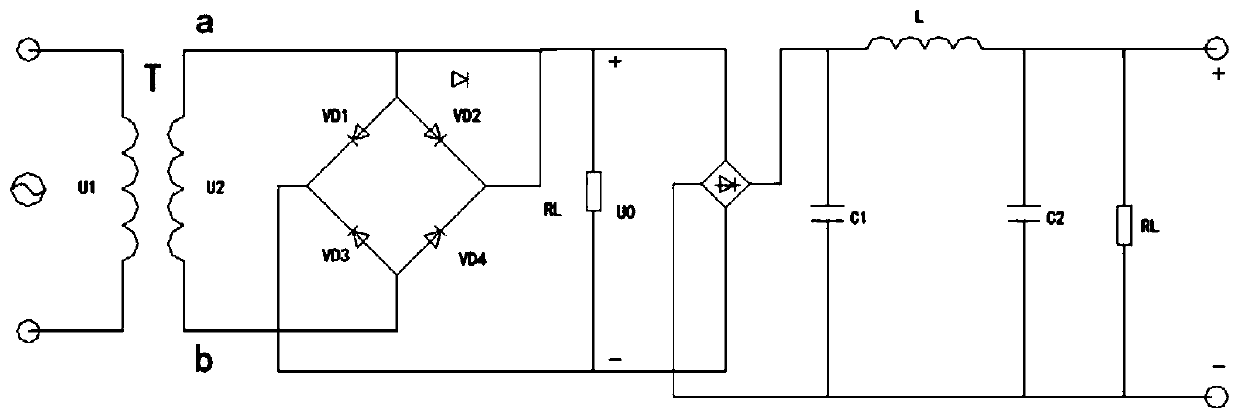
[0040] refer to figure 1 , provides the circuit diagram of the rectification filter circuit of the present invention;
[0041] The rectification filter circuit is composed of a single-phase bridge rectification circuit and an LC-π filter circuit;
[0042] The single-phase bridge rectifier circuit includes: a power transformer, a rectifier diode VD1, a rectifier diode VD2, a rectifier diode VD3, a rectifier diode VD4 and a load resistor RL; wherein the rectifier diode VD1, rectifier diode VD2, rectifier diode VD3, The rectifier diode VD4 forms a rectifier bridge;
[0043] The transformer transforms the AC voltage of the power grid into ...
PUM
 Abstract
Description
Claims
Application Information
PatSnap Eureka turns technology decisions into work you can execute. Powered by our Innovation Knowledge Graph, it runs expert workflows across engineering, life sciences, materials and intellectual property. Get your review-ready output in minutes.


