

A Silicon Controlled Rectifier Structure with Multiple Trigger Channels
A silicon rectifier and trigger channel technology, applied in the field of electronics, can solve the problems of large trigger path resistance, high trigger voltage, long DTSCR trigger time, etc., and achieve the effect of small trigger path resistance, effective ESD protection, and device performance optimization.
- Summary
- Abstract
- Description
- Claims
- Application Information
AI Technical Summary
Problems solved by technology
Method used
Image

Examples
Embodiment 1
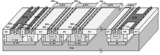
[0026] This embodiment provides a silicon-controlled rectifier structure with multiple trigger channels, and its device structure is as follows image 3 As shown, it consists of a diode string composed of 1 SCR device and n diodes, including:
[0027] The SCR device structure includes: a silicon substrate 100 of the first conductivity type; a deep well region 101 of the second conductivity type formed on the silicon substrate 100 of the first conductivity type, and in the deep well region of the second conductivity type The well region A of the second conductivity type adjacent from left to right formed in 101 1 102. Well region B of the first conductivity type 1 202. Well region A of the second conductivity type 2 302. Well region B of the first conductivity type 2 402 and the second conductivity type well region A 3 502, that is, the first conductivity type well region 202 is surrounded by the second conductivity type well region 102, the second conductivity type deep we...
Embodiment 2
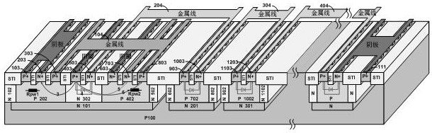
[0037] This embodiment provides a silicon-controlled rectifier structure with multiple trigger channels, and its device structure is as follows Figure 4 As shown, it is composed of a diode string composed of 1 SCR device and n diodes; the difference from Embodiment 1 is that the second conductivity type well region A 2 302 is provided with the second conductivity type heavily doped region D in sequence from left to right 2 503 and the first conductivity type heavily doped region C 3 403, the heavily doped region C of the first conductivity type 3 403 and the second conductivity type heavily doped region D 3 603 is connected to the anode of the device, and the heavily doped region D of the second conductivity type 2 503 is connected to the metal line 204 .
[0038] In this embodiment, compared with the device in Example 1, the improved multi-trigger channel silicon controlled rectifier structure exchanges the p-type heavily doped region 403 and the n-type heavily doped reg...
PUM
 Abstract
Description
Claims
Application Information