Solar cell, preparation method thereof and photovoltaic module
A technology of solar cells and photovoltaic modules, applied in photovoltaic power generation, electrical components, circuits, etc., can solve the problems of reducing photoelectric conversion efficiency of modules, increasing material costs, increasing module area, etc., and achieve the effect of reducing cracks
- Summary
- Abstract
- Description
- Claims
- Application Information
AI Technical Summary
Problems solved by technology
Method used
Image

Examples
Embodiment Construction
[0039] The present invention will be described in detail below in conjunction with the embodiments shown in the accompanying drawings. However, these embodiments do not limit the present invention, and any structural or functional changes made by those skilled in the art according to these embodiments are included in the protection scope of the present invention.
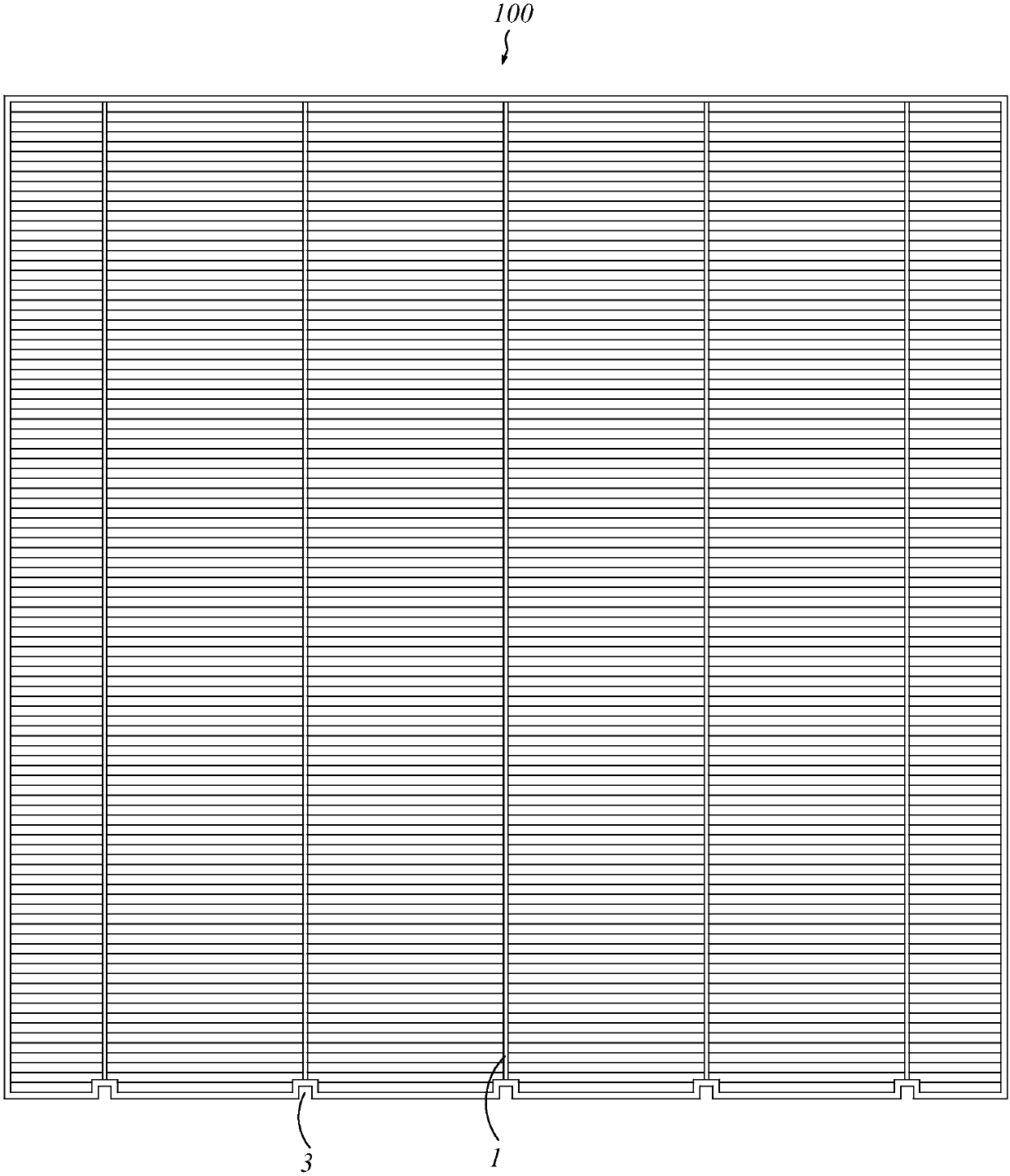
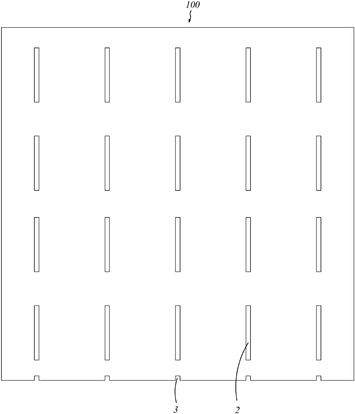
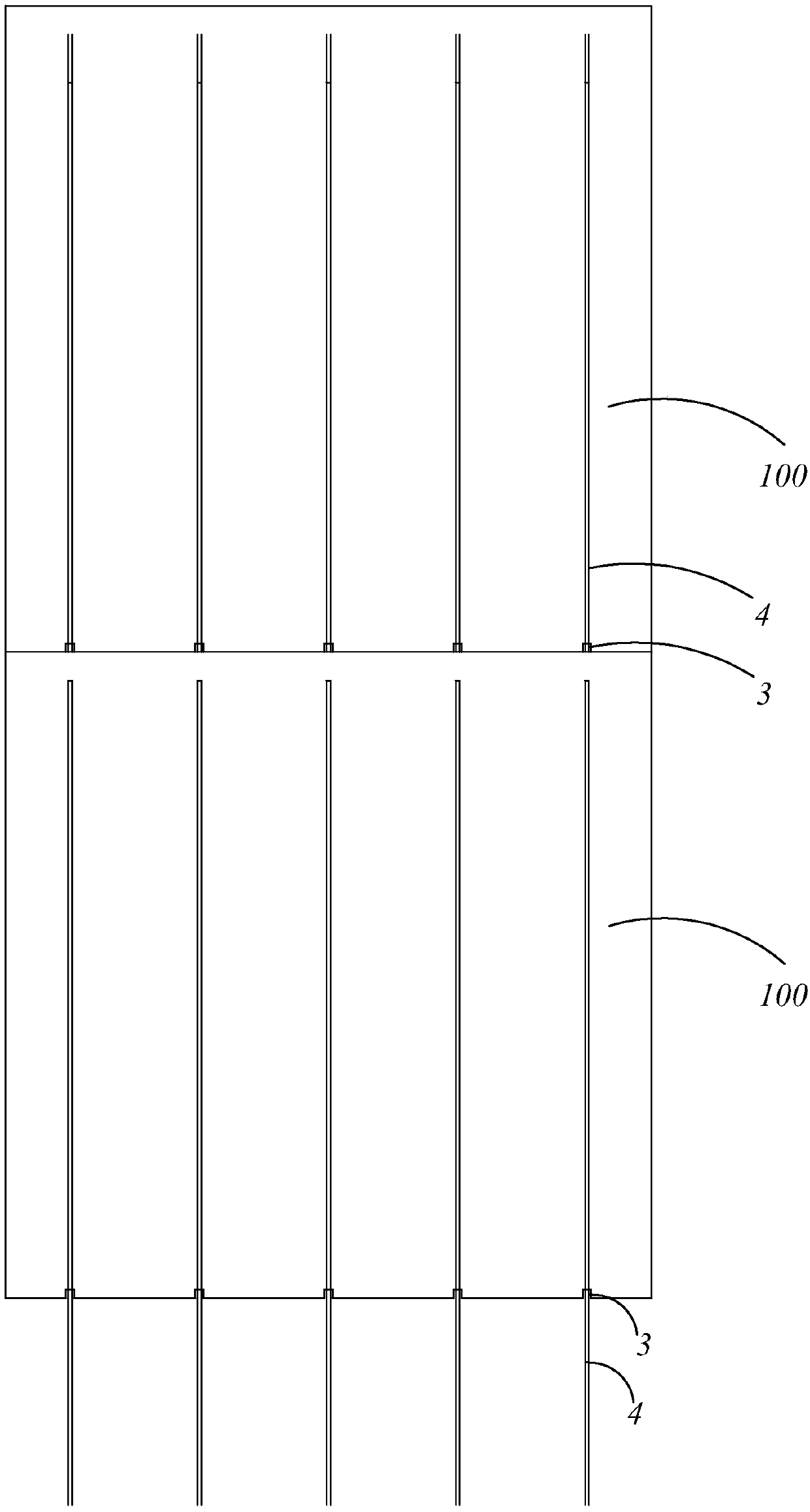
[0040] Such as Figure 1~Figure 10 Shown is a solar battery sheet 100 in a preferred embodiment of the present invention, the surface of the solar battery sheet 100 is provided with several main grids (1, 2), and the edge of the solar battery sheet 100 is provided with several The grid (1, 2) corresponds to the through groove 3. Those skilled in the art can understand that the “several busbars” mentioned above may be part or all of the busbars on the surface of the solar cell 100 .
[0041] By opening the through groove 3 on the edge of the solar battery sheet 100, the crack phenomenon of the solar battery sheet 1...
PUM
 Abstract
Description
Claims
Application Information