

Pressure sensor and preparation method of pressure sensor
A pressure sensor and sensor technology, applied in the sensor field, can solve the problems of difficult mass production, high production process requirements, wear and other problems
- Summary
- Abstract
- Description
- Claims
- Application Information
AI Technical Summary
Problems solved by technology
Method used
Image

Examples
Embodiment 1
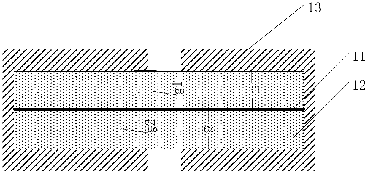
[0036] Schematic diagram of a prior art pressure sensor with reference to figure 1 As mentioned above, the working principle of the pressure sensor is C=εS / d (ε is the dielectric constant, S is the area, and d is the distance). When there is external pressure, the deformable metal sheet (common electrode) 11 will be bent to change the phase Changing the distance between the two capacitances formed by the common electrode 11 and the metal plates on both sides of the metal electrode 13, the difference between the two capacitances will occur immediately, and the greater the external pressure, that is, the greater the gas concentration, the greater the difference between the two capacitances. The structural diagram of the pressure sensor in the prior art is as follows: 12 is the electrolyte, 11 is the common electrode (deformable metal sheet), 13 is the metal electrode, g1 and g2 are the distances between the two capacitors, and C1 and C2 are respectively The capacitance formed by...
Embodiment 2
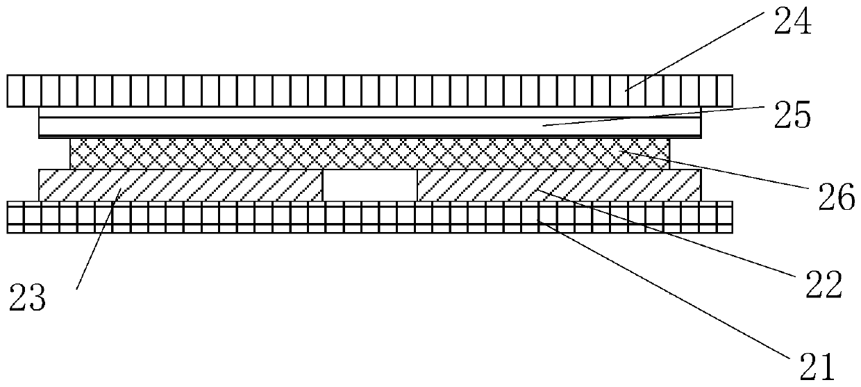
[0059] The embodiment of the present invention discloses a preparation method of a pressure sensor, referring to Figure 6 , the method includes:
[0060] Step 601, providing a first substrate.
[0061] In the embodiment of the present invention, the first substrate may be a glass substrate. When the sensor is a sensor prepared by combining a TFT-LCD manufacturing process with a sensor principle, the first substrate may be a TFT substrate.
[0062] Step 602 , forming a first metal electrode, a second metal electrode, and a first alignment mark on the first substrate.
[0063] In the embodiment of the present invention, a metal layer can be formed on the first substrate by using a film-forming process. Optionally, the material for preparing the metal layer can be one of Mo, Al, and ITO metal. For the The metal layer is exposed to form a preset pattern, and other regions in the metal layer are etched away by an etching process, and the metal in the preset pattern is retained, ...
PUM
 Abstract
Description
Claims
Application Information