Method for determining photoetching process window

A lithography process and exposure unit technology, which is applied to microlithography exposure equipment, pattern surface photoengraving process, photoengraving process exposure device, etc., can solve problems such as affecting wafer exposure quality, avoid errors, improve The effect of productivity

Inactive Publication Date: 2019-12-31
SHANGHAI HUALI INTEGRATED CIRCUTE MFG CO LTD
View PDF5 Cites 3 Cited by
  • Summary
  • Abstract
  • Description
  • Claims
  • Application Information

AI Technical Summary

Problems solved by technology

[0004] The judgment of imaging quality is often related to the experience of the engineer. Judging base

Method used


Image

  • Method for determining photoetching process window
  • Method for determining photoetching process window

Examples


Embodiment Construction

[0024] The technical solutions in the present invention will be clearly and completely described below in conjunction with the accompanying drawings. Apparently, the described embodiments are part of the embodiments of the present invention, not all of them. Based on the embodiments of the present invention, all other embodiments obtained by persons of ordinary skill in the art without making creative efforts belong to the protection scope of the present invention.

[0025] In an embodiment of the present invention, a method for determining a photolithography process window is provided. A method for determining a photolithography process window according to an embodiment of the present invention includes:

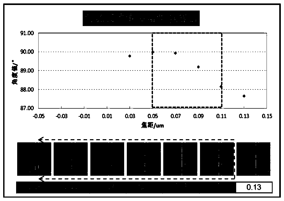
[0026] S1: Provide a wafer, and select various types of graphics on the wafer as the graphics for determining the exposure process window;

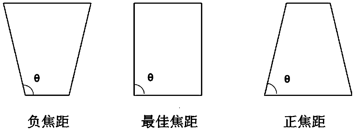
[0027] Specifically, in an embodiment of the present invention, the multiple types of graphics include dense graphics, semi-dense gr...


PUM


Abstract

The invention relates to a method for determining a photoetching process window and relates to the semiconductor integrated circuit process. The method is characterized in that firstly, selecting a plurality of types of graphs as graphs for judging an optimal exposure process window, then setting an energy-focal length matrix during exposure of a photoetching machine, exposing wafers, measuring line widths of the graphs of different exposure units, collecting line width sizes of the selected various types of graphs, forming a Poisson curve according to the line width sizes, removing the energy-focal length matrix corresponding to unreasonable angle data, and thereby accurately determining the optimal process window of photoetching. The method is advantaged in that new products are importedquickly, the production capacity is improved, manual judgment is not needed, and errors caused by manual judgment are avoided.

Description

technical field [0001] The invention relates to semiconductor integrated circuit technology, in particular to a method for determining a photolithography process window. Background technique [0002] From the advent of the first transistor, the development of semiconductor technology has been more than 50 years. According to Moore's law, the chip integration level doubles in 18 months, and the device size shrinks by 0.7 times every three years. Today, it still maintains a strong development With the development of integrated circuits from micron to nanoscale, the wavelength of light used in lithography has also changed from 436nm and 365nm in the near ultraviolet (NUV) range to 248nm and 193nm in the deep ultraviolet (DUV) range. At present, most chip manufacturing processes use 248nm and 193nm lithography technologies. As technology nodes advance, the lithography process window becomes smaller and smaller. [0003] Photolithography is one of the core processes in integrat...

Claims


Application Information

Patent Timeline
IPC IPC(8): G03F7/20
CPCG03F7/70425G03F7/70491
Inventor 高松张聪胡丹丹
Owner SHANGHAI HUALI INTEGRATED CIRCUTE MFG CO LTD
Why Eureka
Try Eureka