Nonvolatile memory processing method and device
A technology of non-volatile memory and processing method, applied in the field of non-volatile memory processing method and device, capable of solving problems such as unstable performance of non-volatile memory
- Summary
- Abstract
- Description
- Claims
- Application Information
AI Technical Summary
Problems solved by technology
Method used
Image
Examples
Embodiment 1
[0034] refer to figure 1 , which shows a flow chart of a non-volatile memory processing method, which may specifically include the following steps:
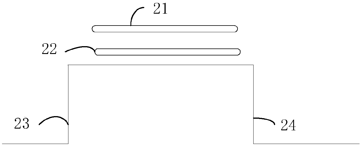
[0035] In the embodiment of the present invention, taking the non-volatile memory NAND Flash as an example, the storage unit of the NAND Flash is as follows figure 2 As shown, the reference number 21 represents the control gate (Control gate, CG); the reference number 22 represents the floating gate (Floating gate, FG); the reference number 23 represents the drain (Drain); and the reference number 24 represents the source (Source).
[0036] When programming a non-volatile memory, by applying a high voltage to the control gate 21 and a low voltage to the drain 23, the electrons in the memory cell channel (Channel) can be written into the floating gate 22, completing programming operation.
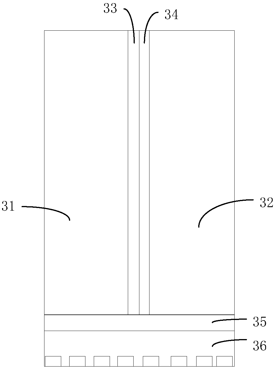
[0037] exist image 3 In, a NAND Flash with a dual plane architecture is shown, image 3 The number 31 represents one of the planes, whic...
Embodiment 2
[0052] refer to Figure 5 , showing a block diagram of a non-volatile memory processing device, the device may specifically include:
[0053] a receiving module 510, configured to receive an operation instruction for the non-volatile memory;
[0054] The control module 520 is configured to simultaneously turn on the control switches corresponding to the plurality of storage boards according to the operation instruction.
[0055] Preferably, the word line WL of each of the planes is connected to the control switch corresponding to each of the planes; each of the control switches controls the start or stop of each of the planes through each of the WLs.
[0056] Preferably, each of the planes also corresponds to: a word line control area, a bit line control area;
[0057] The word line control area is used to control the word line WL voltage of the plane;
[0058] The bit line control area is used to control the voltage of the bit line BL of the plane.
[0059...
PUM
 Abstract
Description
Claims
Application Information


