
Open cavity processing method for protecting PCB inner line by wet film

A technology of inner-layer circuit and processing method, which is applied in multi-layer circuit manufacturing, printed circuit, printed circuit manufacturing, etc., can solve the problems of inner-layer circuit with gold-stained short circuit, interlayer voids, poor reliability, and false filling, etc., to achieve Strengthen the significance of promotion, ensure cleanliness, and avoid the effect of waste residue

Active Publication Date: 2020-01-14
东莞康源电子有限公司
View PDF7 Cites 0 Cited by
  • Summary
  • Abstract
  • Description
  • Claims
  • Application Information

AI Technical Summary

Problems solved by technology

[0003] For this reason, the main purpose of the present invention is to provide a method of opening cavity using nickel or tin to protect PCB inner layer circuit, so as to solve the problem of traditional circuit board cavity opening with gold-stained inner layer circuit short circuit, waste residues that are not easy to fall off, glue flow, and false filling. , interlayer voids and poor reliability

Method used


Image

  • Open cavity processing method for protecting PCB inner line by wet film
  • Open cavity processing method for protecting PCB inner line by wet film

Examples


Embodiment Construction

[0022] In order to make the object, technical solution and advantages of the present invention clearer, the present invention will be further described in detail below in conjunction with the accompanying drawings and embodiments.

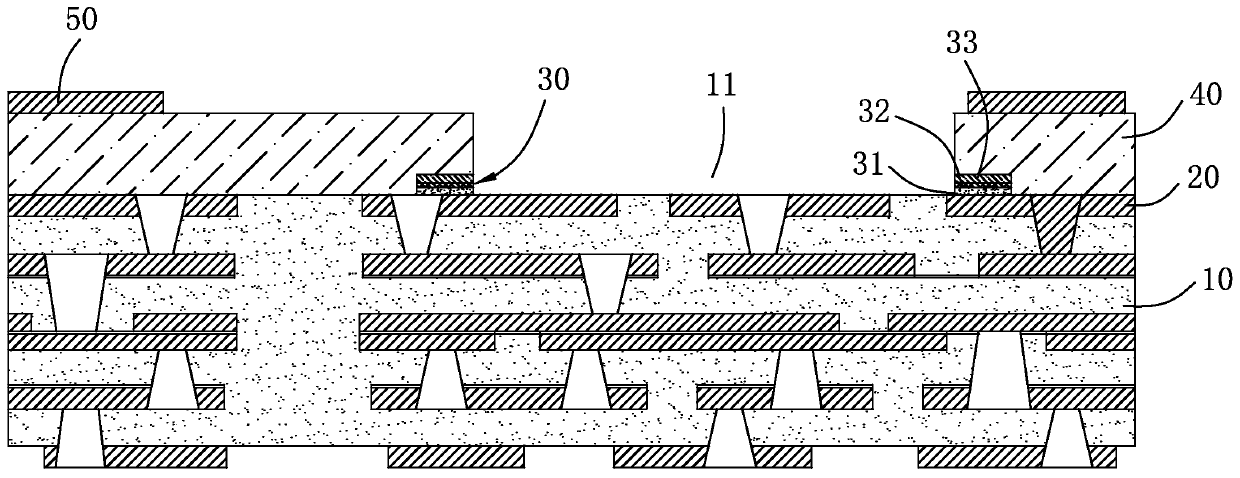
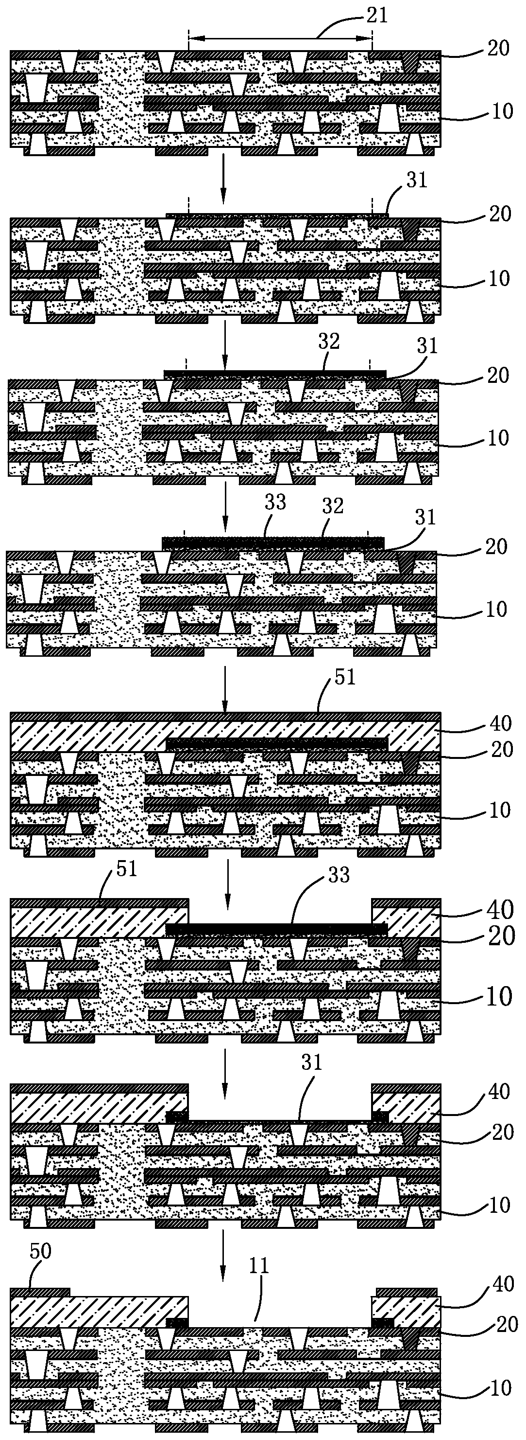
[0023] Such as figure 1 with figure 2 As shown, the present invention provides a cavity opening processing method using a wet film to protect the inner layer circuit of the PCB, which is used for cavity opening processing outside the inner layer circuit of the PCB. The PCB includes an inner layer 10 , an inner layer circuit 20 , a protective layer 30 , an outer layer 40 and an outer layer circuit 50 . The inner layer 10 is a conventional multilayer board, and the inner layer circuit 20 is disposed on the inner layer 10 . The protective layer 30 is disposed on the outer surface of the inner circuit 20 , the outer layer 40 covers the outer surface of the protective layer 30 , and the outer circuit 50 is disposed on the outer surface of the outer la...


PUM


Abstract

The invention relates to an open cavity processing method for protecting a PCB inner line by a wet film. The method comprises the following steps: step 1, manufacturing an inner line on the inner layer; step 2, covering the outer surface of the inner line with a wet film layer; step 3, forming a metal film layer on the outer side of the wet film layer; step 4, coating a copper layer on the outer side of the metal film layer; step 5, pressing an outer layer on the outer side of the copper layer and arranging an outer copper layer on the outer surface of the outer layer; step 6, performing laserslotting on the outer surface of the copper layer of the protective layer to enable the copper layer on the protective layer to be exposed; step 7, adopting the etching process to perform etching treatment on the outer copper layer to form an outer line and simultaneously etching off the copper layer at the bottom of the slot; and step 8,removing the wet film layer at the bottom of the slot. Theopen cavity processing method can ensure the cleanliness inside the cavity body and avoid the problems of waste residue in the cavity body, short circuit caused by gold stain, glue flow, false fillingand interlayer holes. The method has high practicability and high popularization significance.

Description

technical field [0001] The invention relates to a circuit board processing method, in particular to a cavity opening processing method using a wet film to protect the PCB inner layer circuit. Background technique: [0002] Some current PCBs are provided with inner-layer circuits, and cavities / blind slots are provided on the PCB outside the inner-layer circuits. However, after the traditional PCB is opened, there are problems such as low cleanliness in the cavity, glue traces or resin or other waste residues in the cavity, and it is not easy to fall off. And the cavity / blind groove is usually carried out after the final surface treatment of the PCB; and in the ENIG (Electroless Nickel Immersion Gold, electroless nickel immersion gold) process or ENEPIG (Electroless Nickel Electroless Palladium Immersion Gold, electroless nickel plating palladium immersion gold) process Finally, the gap between the lines in the cavity is easy to be stained with gold and cause a short circuit....

Claims


Application Information

Patent Timeline
Patent Type & Authority Applications(China)
IPC IPC(8): H05K3/46
CPCH05K3/4697
Inventor 杜军李明军邓贤江
Owner 东莞康源电子有限公司
Learn More