Backlight source and manufacturing method thereof, backlight module, display panel and display device

A manufacturing method and backlight module technology are applied in the fields of backlight modules, backlight sources and manufacturing methods, display devices, and display panels, and can solve the problems of large Mini LED area, increased difficulty in display algorithms, and increased device thickness, etc., so as to achieve luminous light The effect of reducing halo, improving light energy utilization efficiency, and reducing diffusion

Pending Publication Date: 2020-01-24
BOE TECH GRP CO LTD +1
View PDF5 Cites 14 Cited by
  • Summary
  • Abstract
  • Description
  • Claims
  • Application Information

AI Technical Summary

Problems solved by technology

[0003] Mini LED is used as a backlight device, and there are gaps between the Mini LEDs. In order to cover the differences between the Mini LEDs, it is necessary to use a diffusion film and a certain mixing distance to perfectly cover them, which indirectly increases the device’s At the same time, due to the use of diffusion and other materials, the Mini LED ligh

Method used


Image

  • Backlight source and manufacturing method thereof, backlight module, display panel and display device
  • Backlight source and manufacturing method thereof, backlight module, display panel and display device
  • Backlight source and manufacturing method thereof, backlight module, display panel and display device

Examples


Embodiment Construction

[0041] In order to illustrate the present invention more clearly, the present invention will be further described below in conjunction with preferred embodiments and accompanying drawings. Similar parts in the figures are denoted by the same reference numerals. Those skilled in the art should understand that the content specifically described below is illustrative rather than restrictive, and should not limit the protection scope of the present invention.

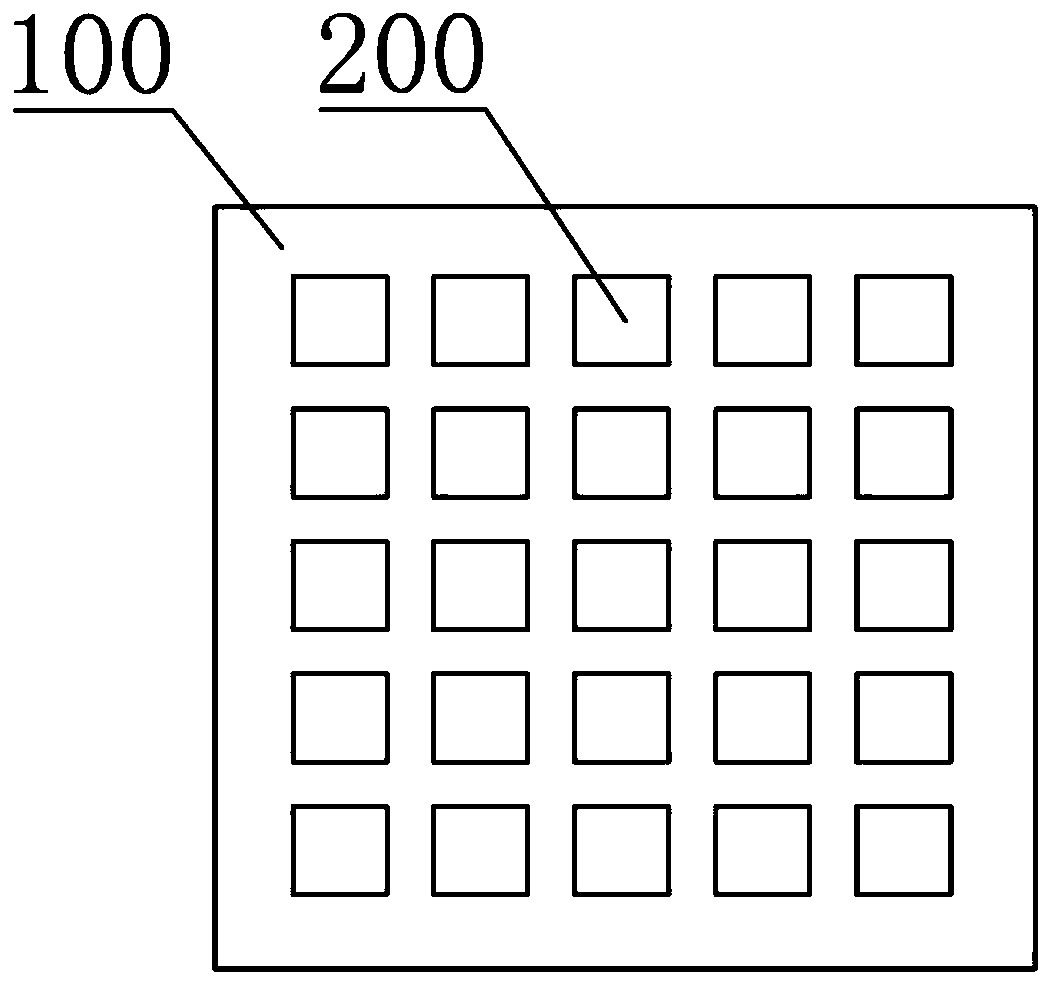
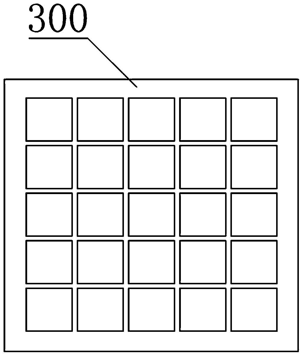
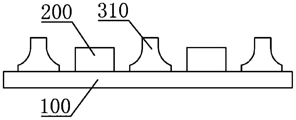
[0042] An embodiment of the present invention provides a backlight, including: a substrate 100 , a plurality of light emitting units 200 and a mesh 300 .

[0043] specific, figure 1 A schematic structural view showing the substrate 100 and the light emitting unit 200 in this embodiment, figure 2 Shown as a schematic structural diagram of the mesh member 300, in figure 1 In an example, the substrate 100 can be a circuit board, and a plurality of light-emitting units 200 are arranged on the substrate 100 at intervals. f...


PUM


Abstract

The invention discloses a backlight source, comprising: a substrate; a plurality of light emitting units disposed on the substrate at intervals; and a mesh member comprising a plurality of hollow structures in one-to-one correspondence to the plurality of light emitting units, wherein the plurality of hollow structures of the mesh member are arranged on the plurality of light emitting units in a sleeving manner one by one, a reflection structure is arranged on the mesh member, and the reflection structure is used for reflecting the light emitted from a side light emitting surface of each lightemitting unit, so that the reflected light is gathered in a direction perpendicular to the surface of the substrate. The backlight source disclosed by the invention can effectively utilize the lightemitted from the side light emitting surfaces of the light emitting units, thereby improving the utilization efficiency of light energy. At the same time, by adjusting the light emitting type of the light emitting units, the light mixing distances of the light emitting units can be effectively reduced, thereby reducing the thickness of the device, correspondingly reducing the light emitting halo of each light emitting unit, that is, limiting the size of a PSF curve of each light emitting unit, which is beneficial to the adjustment of a display algorithm.

Description

technical field [0001] The invention relates to the field of display technology. More specifically, it relates to a backlight source and a manufacturing method, a backlight module, a display panel, and a display device. Background technique [0002] The application of Mini LED in the field of display is a hot topic in the market in recent years. Mini LED backlight adopts array-type distribution of Mini LED to achieve high contrast effect of display technology by locally controlling the brightness of Mini LED. At the same time, Mini LED backlight , using the technology of blue light to excite quantum dots to produce white light, a wide color gamut effect is obtained, which greatly shortens the distance from OLED, so that LED can regain its advantage in comparison with OLED. [0003] Mini LED is used as a backlight device, and there are gaps between the Mini LEDs. In order to cover the differences between the Mini LEDs, it is necessary to use a diffusion film and a certain mi...

Claims


Application Information

Patent Timeline
IPC IPC(8): G02F1/13357G09F9/30
CPCG02F1/133603G02F1/133605G02F1/133611G09F9/30
Inventor 汪志强王雪绒孙川陈雷马鑫王秋里杨超姚建峰芮博超时凌云
Owner BOE TECH GRP CO LTD
Why Eureka
Try Eureka