

Universal Device for Ball Grid Array Device Planting
A ball grid array and general-purpose device technology, which is applied in the manufacturing of semiconductor devices, electric solid-state devices, and semiconductor/solid-state devices, etc., can solve the problems of high operator requirements, delayed production schedule, and missing solder balls, and achieves a simple structure of the device. Realize the effect of fast missing installation and improve production efficiency
- Summary
- Abstract
- Description
- Claims
- Application Information
AI Technical Summary
Problems solved by technology
Method used
Image

Examples
Embodiment Construction
[0027] The preferred embodiments of the present invention will be described in detail below in conjunction with the accompanying drawings.
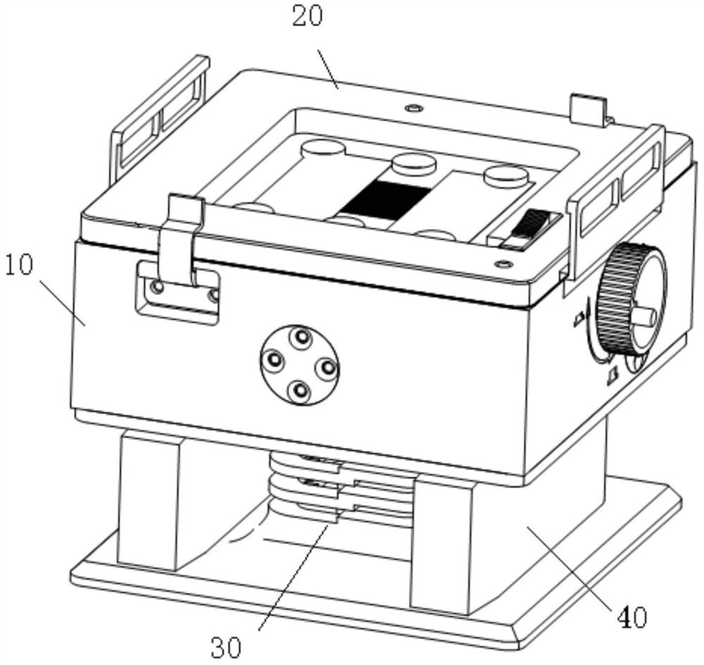
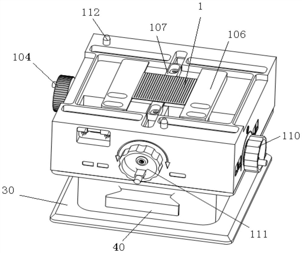
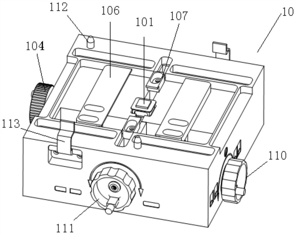
[0028] refer to Figure 1-Figure 9 As shown, in the preferred embodiment described below, a general device for planting balls of ball grid array devices includes: a general solder ball drain plate 20 installed above the ball planting table 10, an elastic base 30 below the ball planting table 10 and The U-shaped card slot is characterized in that: the central part of the ball planting pool of the inner cavity frame of the ball planting table 10 is provided with a lifting support block 101 that drives and places the ball grid array device substrate 1 on it to rise / fall synchronously, and the height distance is adjustable. The lifting support block 101 is symmetrical, the auxiliary clamping slider 107 that slides along the wide-side suspension beam slide rail, and the main clamping slider 106 that slides along the chute on both sides of the ...
PUM
 Abstract
Description
Claims
Application Information