High-sensitivity vertical magnetic field sensor with symmetrical structure

A magnetic field sensor and high-sensitivity technology, applied in the direction of the size/direction of the magnetic field, Hall effect devices, and the manufacture/processing of electromagnetic devices, can solve the development requirements that cannot meet the low cost and high integration of magnetic field sensor microsystems, Can not be compatible with silicon-based process, increase production costs and other issues, to achieve the effect of low initial offset, low production cost, and eliminate offset

Active Publication Date: 2020-01-31
NANJING UNIV OF POSTS & TELECOMM
View PDF6 Cites 1 Cited by
  • Summary
  • Abstract
  • Description
  • Claims
  • Application Information

AI Technical Summary

Problems solved by technology

However, this method requires additional processing of the magnetic field concentrator, which increases the production cost and is prone to the disadvantage of magnetic field distortion
At present, new anisotropic magnetoresistance (AMR), giant magnetoresistance (GMR), giant magnetoresistance (GMI) and other magnetic field elements show high magnetic field sensitivity and good temperature stability, but they cannot be compared with silicon-based processes. Very good compatibility, but still unable to meet the development requirements of low-cost and high-integration magnetic field sensor microsystems
[0004] At present, low-cost two-dimensional and three-dimensional integrated Hall magnetic sensors based on deep submicron standard silicon-based CMOS technology have serious problems of low magnetic field sensitivity and high offset, especially the extremely low magnetic field sensitivity and non-magnetic field sensitivity of traditional vertical Hall devices. The fully symmetrical device structure has become the biggest bottleneck restricting the development and application of low-cost 2D and 3D integrated Hall sensors

Method used


Image

  • High-sensitivity vertical magnetic field sensor with symmetrical structure
  • High-sensitivity vertical magnetic field sensor with symmetrical structure
  • High-sensitivity vertical magnetic field sensor with symmetrical structure

Examples


Embodiment Construction

[0023] Objects, advantages and features of the present invention will be illustrated and explained by the following non-limiting description of preferred embodiments. These embodiments are only typical examples of applying the technical solutions of the present invention, and all technical solutions formed by adopting equivalent replacements or equivalent transformations fall within the protection scope of the present invention.

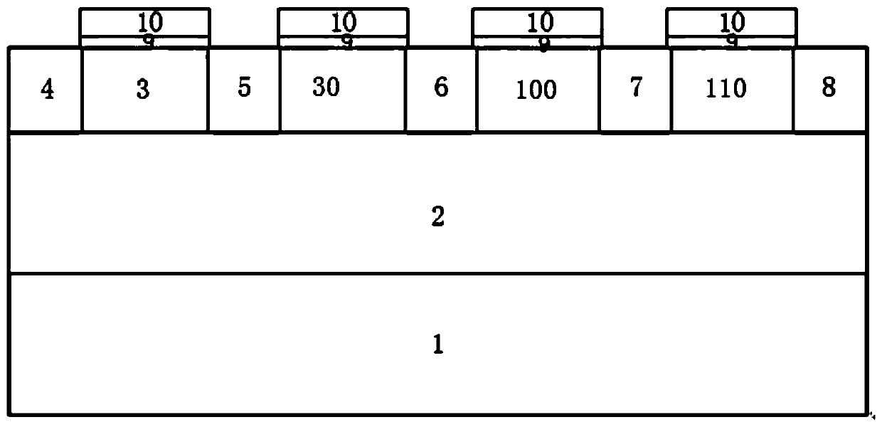
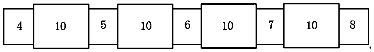
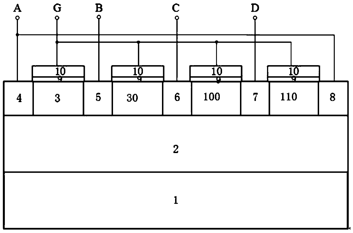
[0024] The present invention discloses a high-sensitivity vertical magnetic field sensor with a symmetrical structure, including a first vertical magnetic field sensor and a second vertical magnetic field sensor arranged vertically symmetrically, such as figure 1 and figure 2 As shown, the first vertical magnetic field sensor and the second vertical magnetic field sensor share the third N+ region 6 .

[0025] The magnetic field sensor includes a silicon substrate 1, an insulator layer 2, a first P-region 3, a second P-region 30, a third P-region 10...


PUM

PropertyMeasurementUnit
thicknessaaaaaaaaaa
thicknessaaaaaaaaaa

Abstract

The invention discloses a high-sensitivity vertical magnetic field sensor with a symmetrical structure. The magnetic field sensor comprises a first vertical magnetic field sensor and a second verticalmagnetic field sensor, which are vertically and symmetrically arranged, wherein the first vertical magnetic field sensor and the second vertical magnetic field sensor share a third N + region. The magnetic field sensor comprises a silicon substrate, an insulator layer, a first P-region, a second P- region, a third P- region, a fourth P- region, a first N + region, a second N + region, a third N +region, a fourth N + region, a fifth N + region, a gate dielectric layer and a gate. The magnetic field sensor with the symmetrical structure has a simple production process, a completely symmetricalstructure and low initial device offset, furthermore, the device offset can be eliminated by using the rotating current technology, and the residual offset is low. The vertical magnetic field sensorhas high magnetic field sensitivity, and can form a two-dimensional magnetic field sensor to realize the detection of a two-dimensional magnetic field parallel to a device plane.

Description

technical field [0001] The invention relates to a high-sensitivity vertical magnetic field sensor with a symmetrical structure, which can be used in the technical field of electromagnetic detection. Background technique [0002] The vertical magnetic field sensor can detect the magnetic field parallel to the surface of the device to form a two-dimensional (2D) and three-dimensional (3D) magnetic field sensor to realize functions such as precise position positioning, small displacement measurement, rotational movement, current detection and angle measurement. In recent years, vertical Hall magnetic field sensors with low-cost silicon-based technology have been widely used in many fields such as automatic control, automobiles, medical equipment, intelligent instruments and meters, and consumer electronics. Traditional silicon-based CMOS vertical Hall devices such as five-hole and six-hole structures, although the device structure is simple, the initial misalignment of the devi...

Claims


Application Information

Patent Timeline
Patent Type & Authority Applications(China)
IPC IPC(8): G01R33/02H01L43/06H01L43/14
CPCG01R33/02H10N52/00H10N52/01
Inventor 徐跃宋福明袁丰
Owner NANJING UNIV OF POSTS & TELECOMM
Why Eureka
Try Eureka