Wafer detection device, wafer transfer system and wafer detection method

A detection device, wafer technology, applied in the direction of semiconductor/solid-state device testing/measurement, electrical components, circuits, etc., can solve the problems of wafer detection errors, tilt, etc.

Active Publication Date: 2020-02-04
BEIJING NAURA MICROELECTRONICS EQUIP CO LTD
View PDF5 Cites 0 Cited by
  • Summary
  • Abstract
  • Description
  • Claims
  • Application Information

AI Technical Summary

Problems solved by technology

[0006] The application provides a wafer detection device, a wafer transmission system and a wafer detection method to solve the current problem of wafer detection errors due to the inclination of the laser path

Method used


Image

  • Wafer detection device, wafer transfer system and wafer detection method
  • Wafer detection device, wafer transfer system and wafer detection method
  • Wafer detection device, wafer transfer system and wafer detection method

Examples


Embodiment 1

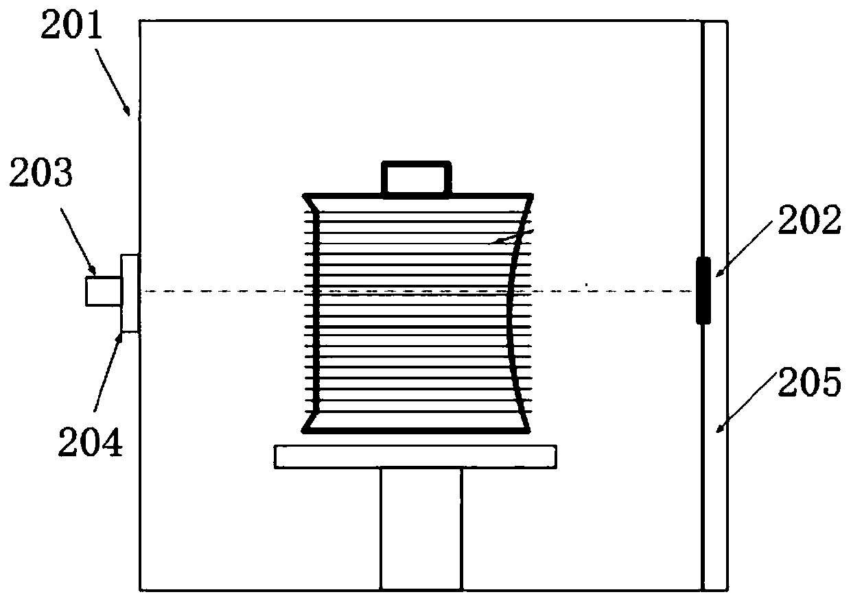
[0044] refer to figure 2 , which shows a schematic structural view of a wafer detection device described in Embodiment 1 of the present application. The wafer detection device is arranged on the loading chamber 201, and specifically includes:

[0045] Reflecting plate 202 , transceiver 203 and fixing plate 204 .

[0046] The fixing plate 204 is installed on the side wall of the loading chamber 201 , and the fixing plate 204 is provided with a light hole.

[0047] In practical applications, a wafer box may also be provided in the loading chamber, and the wafer box is used for placing wafers.

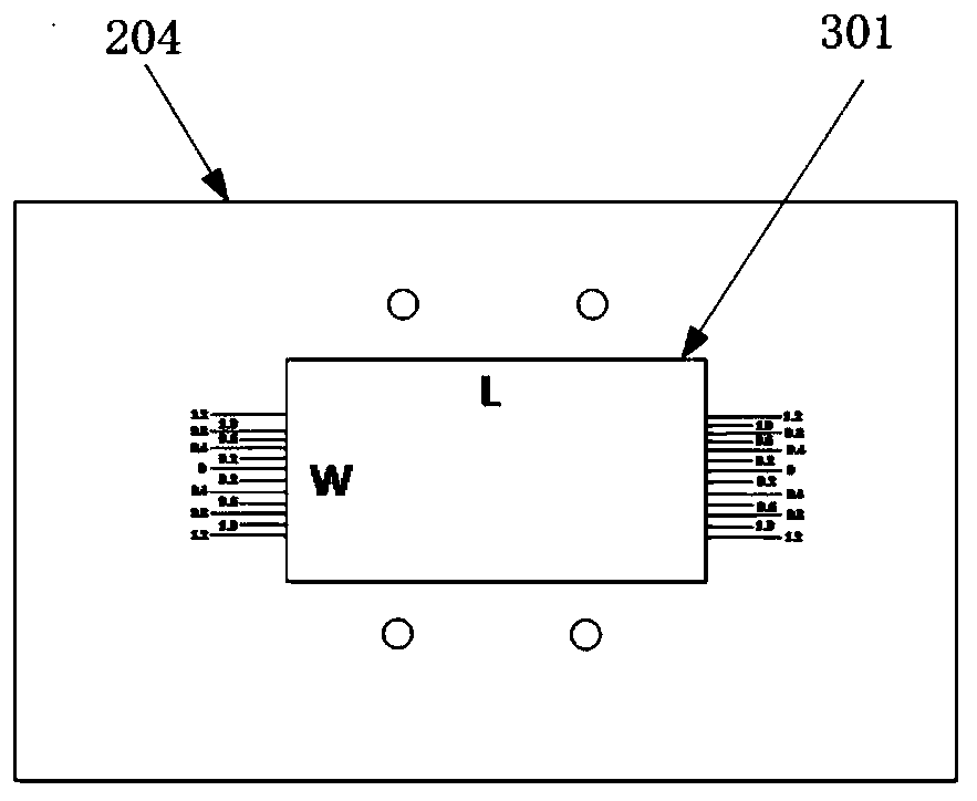
[0048] exist image 3 The figure shows the positions of the fixing plate 204 and the light hole 301. The light hole 301 is set at the middle position of the fixing plate 204, and can also be set at other positions, which is not specifically limited in this application.

[0049] The transceiver 203 is mounted on the fixing plate 204, and the transceiver 203 emits laser light into the l...

Embodiment 2

[0071] The present application also discloses a wafer transmission system, including the wafer detection device in the first embodiment.

[0072] And the loading chamber is also provided with a lifting platform and a servo motor.

[0073] Lift table for placing wafer cassettes.

[0074] The servo motor is used to control the movement of the lifting table according to the position of the wafer cassette.

[0075] In practical applications, the servo motor can be connected to the lifting platform through a rotating shaft, so that the servo motor can control the movement of the lifting platform according to the position information of the wafer cassette.

[0076] The wafer transmission system has all the advantages of the wafer inspection device in the first embodiment above, and will not be repeated here.

Embodiment 3

[0078] refer to Figure 7 , which shows a flow chart of a wafer detection method described in Embodiment 3 of the present application, the method is applied to a wafer transmission system, and specifically includes:

[0079] Step 701: loading the wafer into the loading chamber.

[0080] Step 702: The servo motor controls the wafer box of the lifting platform to be at the initial position of wafer detection.

[0081] Step 703: The transceiver emits laser light into the loading chamber through the light hole, and receives reflected light reflected by the reflector through the light hole.


PUM

PropertyMeasurementUnit
widthaaaaaaaaaa

Abstract

The present application provides a wafer detection device, a wafer transfer system and a wafer detection method. The device is disposed on a loading chamber, and includes a reflection plate, a transceiver and a fixing plate. The fixing plate is mounted on a side wall of the loading chamber. A light passing hole is disposed on the fixing plate. The transceiver is mounted on the fixing plate. The transceiver emits laser into the loading chamber through the light passing hole. Reflected light of the laser is received through the light passing hole. The reflection plate is mounted on an outer doorof the loading chamber. The side wall is disposed opposite the outer door. The reflection plate is disposed opposite the light passing hole. The reflection plate is used to reflect the laser emittedby the transceiver. According to the reflected light received by the transceiver through the light passing hole, a controller determines whether a wafer is present at a predetermined position in the loading chamber. Therefore, the problem of wafer detection errors is solved.

Description

technical field [0001] The present application relates to the technical field of semiconductors, in particular to a wafer inspection device, a wafer transmission system and a wafer inspection method. Background technique [0002] The wafer transfer system is an important part of semiconductor special equipment. The wafer transfer system is responsible for the fast, efficient and reliable transfer of wafers between different process modules. [0003] Existing wafer inspection structures such as figure 1 As shown, it specifically includes: a loading chamber 101 , a receiving sensor 102 , a transmitting sensor 103 , and an outer door 104 . The receiving sensor 102 is fixed on the side wall of the loading chamber 101 , and the transmitting sensor 103 is installed on the intermediate adjustment bracket inside the outer door 104 of the loading chamber 101 . [0004] When the chip is tested and debugged, it is necessary to remove the protective plate outside the outer door, and r...

Claims


Application Information

Patent Timeline
Patent Type & Authority Applications(China)
IPC IPC(8): H01L21/67H01L21/66
CPCH01L21/67253H01L22/24
Inventor 商家强
Owner BEIJING NAURA MICROELECTRONICS EQUIP CO LTD
Why Eureka
Try Eureka