Layout structure and formation method of semiconductor integrated circuit device

A technology of layout structure and integrated circuit, which is applied in semiconductor/solid-state device manufacturing, circuits, electrical components, etc., and can solve the problems of large contact resistance, small distance, and difficult preparation of node contact layer 1c.

Pending Publication Date: 2020-02-07
CHANGXIN MEMORY TECH INC
View PDF0 Cites 6 Cited by
  • Summary
  • Abstract
  • Description
  • Claims
  • Application Information

AI Technical Summary

Problems solved by technology

[0008] However, if Figure 1b As shown, since the ends of a plurality of strip-shaped sub-film layers 1b are aligned and arranged, the distance between the adjacent ends of adjacent strip-shaped sub-film layers 1b is relatively small, thereby correspondingly limiting the distance formed on the ends. The size of the node contact layer 1c will easily lead to a large contact resistance between the node contact layer 1c and the strip-shaped sub-film layer 1b; and the process window reserved for the preparation of the node contact layer 1c is small, so that not only the The preparation of the node contact layer 1c is very difficult, and it is also very easy to cause the problem of short-circuiting between the node contact layer 1c and the adjacent strip-shaped sub-film layer 1b

Method used


Image

  • Layout structure and formation method of semiconductor integrated circuit device
  • Layout structure and formation method of semiconductor integrated circuit device
  • Layout structure and formation method of semiconductor integrated circuit device

Examples


Embodiment 1

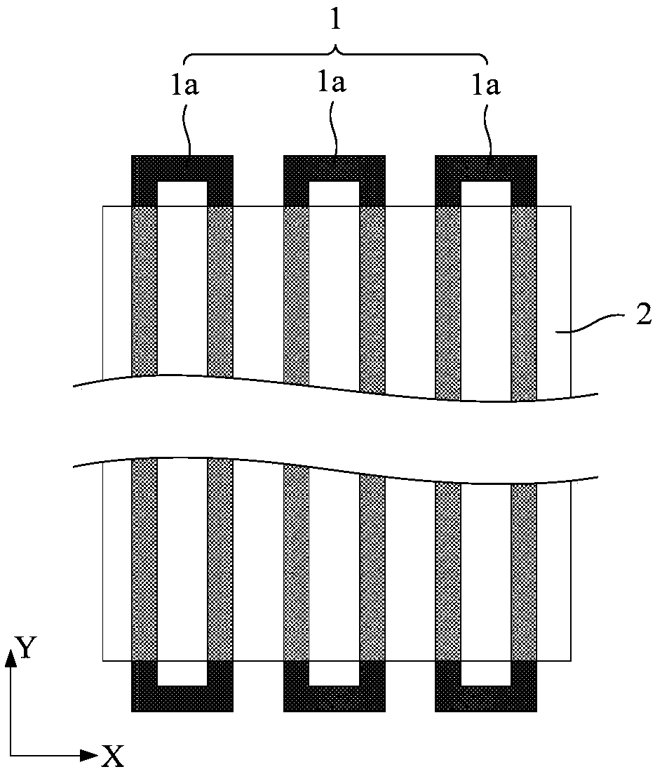
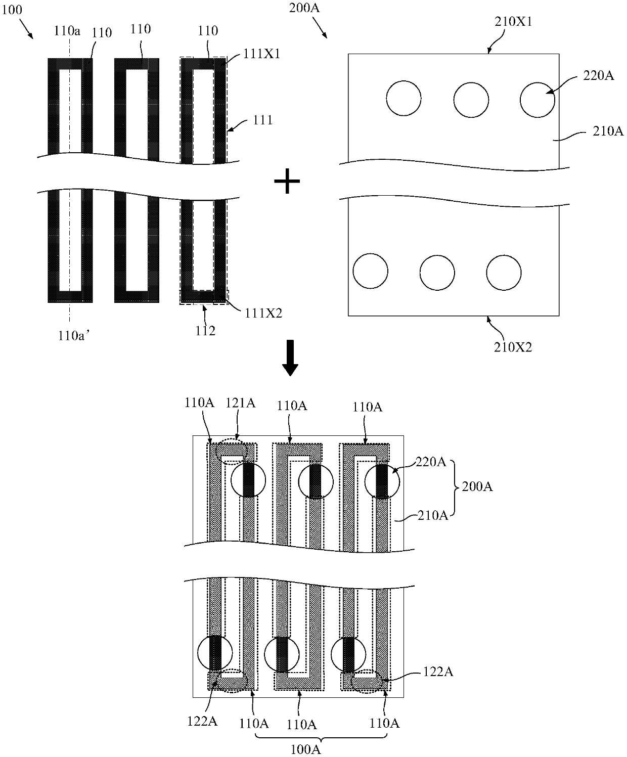
[0113] figure 2 It is a schematic diagram of the layout structure in Embodiment 1 of the present invention, such as figure 2 As shown, the layout includes:

[0114] A first pattern of features 100 comprising at least one first sub-pattern; and,

[0115] The mask pattern 200A has a cover pattern area 210A and a plurality of truncated pattern areas 220A; the cover pattern area 210A has two opposite first borders 210X1 and second borders 210X2 in the second direction (Y direction), the Both the first boundary 210X1 and the second boundary 210X2 extend along the first direction (X direction); and, a plurality of the truncated pattern areas 220A are respectively arranged in regions close to the first boundary 210X1 and the second boundary 210X2.

[0116] It can be understood that, in the photolithography process, the mask pattern area 210A of the mask pattern 200A covers the part that does not need to be exposed, and the cut-off pattern area 220A exposes the part that needs to ...

Embodiment 2

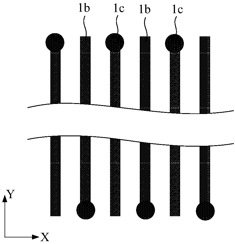
[0147] Figure 4 It is a schematic structural diagram of the layout structure in Embodiment 2 of the present invention. combine figure 2 and Figure 4 As shown, the difference between this embodiment and the first embodiment is that the truncated pattern area of ​​the mask pattern is a non-closed truncated pattern area.

[0148] Such as Figure 4 As shown, the first characteristic pattern 100 in this embodiment has a plurality of annular sub-patterns 110 . And, in the mask pattern 200B, the truncated pattern area 220B is located on the first boundary 210X1 or the second boundary 210X2 of the covering pattern area 210B, and is separated from the first boundary 210X1 or the second boundary 210X2. The boundary 210X2 extends toward the center of the covered graphic area 210B, so that the truncated graphic area 220B is embedded into the covered graphic area 210B from the first boundary 210X1 or the second boundary 210X2. The truncated graphic areas 220B communicate with each ...

Embodiment 3

[0161] In this embodiment, the truncated pattern area of ​​the mask pattern is also a non-closed truncated pattern area. And compared with the second embodiment, the truncated pattern area in this embodiment further exposes all the connection parts of the ring sub-patterns.

[0162] Figure 6a It is one of the structural schematic diagrams of the layout structure in Embodiment 3 of the present invention, such as Figure 6a As shown, in the mask pattern 200C, each of the truncated pattern regions 220C exposes the end of one of the lines 111 of the annular sub-pattern 110, and the plurality of truncated pattern regions 220C are far away from the mask pattern region. One side communicates with each other and further exposes all the connection portions 112 of the annular sub-pattern 110 . That is, the masking pattern area 210C of the mask pattern 200C only covers the lines 111 of the annular sub-pattern 110 , so that the strip-shaped sub-pattern 110C in the second feature patter...


PUM


Abstract

The invention provides a layout structure and a formation method of a semiconductor integrated circuit device. A mask pattern has multiple truncated diagram areas, the multiple truncated diagram areasare close to a boundary covering the diagram areas, so that when a first characteristic pattern is defined as a second characteristic pattern by using the mask pattern, the defined second characteristic pattern can have an edge part close to the truncated diagram areas, and the edge part has a large blank area between a side facing the truncated pattern areas and other parts of an adjacent secondcharacteristic pattern, therefore, when a node area is defined on the edge part of the second characteristic pattern, correspondingly, a larger space area is reserved for the node area, so that corresponding preparation process to be conducted on the node area in later stage is less difficult, and process windows of related processes are increased.

Description

technical field [0001] The invention relates to the technical field of semiconductor integrated circuits, in particular to a layout structure and a method for forming a semiconductor integrated circuit device. Background technique [0002] With the continuous development of semiconductor integrated circuits, it is generally expected to increase the integration density of feature film layers by reducing the size of each feature film layer in the integrated circuit and reducing the distance between adjacent feature film layers. However, with the increasing density of the characteristic film layers, it is more difficult to perform further processing on the formed characteristic film layers with smaller dimensions, so that defects are more likely to occur. [0003] Figure 1a and Figure 1b It is a structural schematic diagram during the preparation process of an existing method for forming a semiconductor integrated circuit device. The forming method includes: [0004] First...

Claims


Application Information

Patent Timeline
Patent Type & Authority Applications(China)
IPC IPC(8): H01L21/027
CPCH01L21/027
Inventor 不公告发明人
Owner CHANGXIN MEMORY TECH INC
Why Eureka
Try Eureka