A packaging process of nox sensor chip
A sensor chip and packaging process technology, applied in instruments, measuring devices, scientific instruments, etc., can solve the problems of chip pollution, sensor chip detection and positioning, no connection structure, etc., to improve the packaging success rate, optimize the packaging process, and prolong the use. effect of life
- Summary
- Abstract
- Description
- Claims
- Application Information
AI Technical Summary
Problems solved by technology
Method used
Image
Examples
Embodiment Construction
[0021] The following will clearly and completely describe the technical solutions in the embodiments of the present invention with reference to the accompanying drawings in the embodiments of the present invention. Obviously, the described embodiments are only some, not all, embodiments of the present invention.
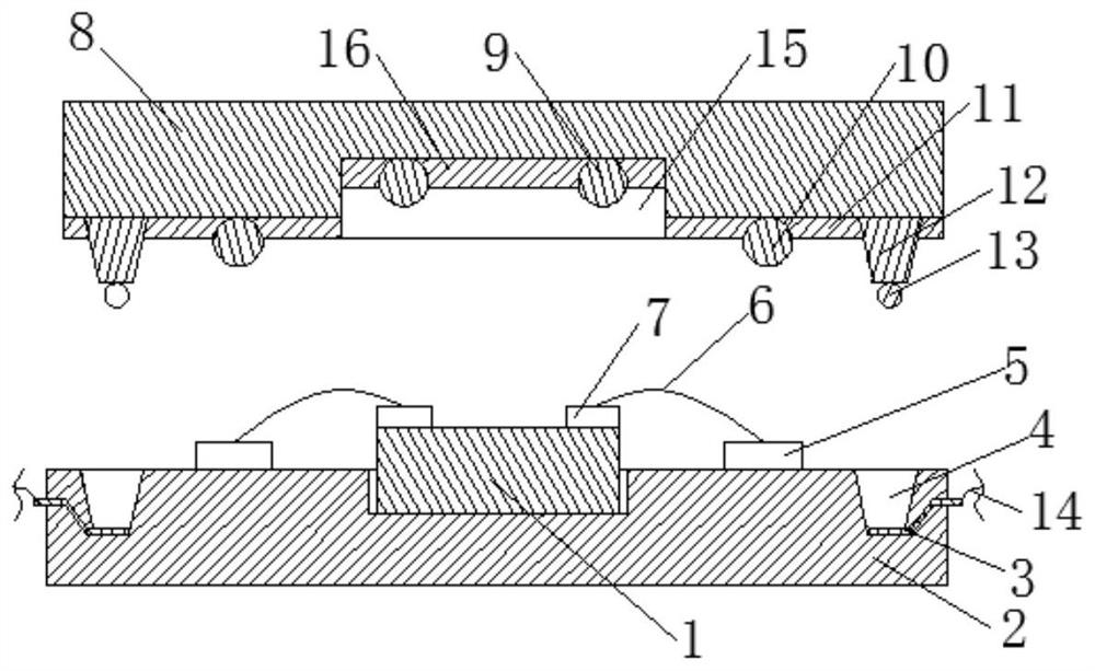
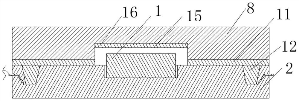
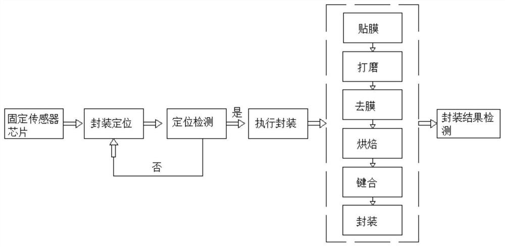
[0022] refer to Figure 1-3 , a NOX sensor chip packaging process, including a substrate 2, a sensor chip 1 is arranged in the substrate 2, a second pad 5 is symmetrically fixed on the left and right sides of the upper surface of the substrate 2, and the left and right sides of the upper surface of the sensor chip 1 are symmetrically arranged. The third pad 7, the second lead 6 is fixed on the upper surface of the third pad 7, the second pad 5 is connected with the third pad 7 through the second lead 6, and the left and right sides of the upper surface of the substrate 2 are provided with connecting grooves 4. A first pad 3 is provided in the connection groove 4, and...
PUM
 Abstract
Description
Claims
Application Information


