Novel electrode configuration structure used for nanometer-level phase change memory unit

A technology of phase change memory and configuration structure, applied in the field of microelectronics, can solve the problems of large difference in resistance between two phases, inability to read, large difference in amorphous resistance, etc., to reduce the equivalent resistance R and facilitate correct reading. Take and suppress the effect of size reduction

Active Publication Date: 2020-02-07
HUAZHONG UNIV OF SCI & TECH
View PDF6 Cites 0 Cited by
  • Summary
  • Abstract
  • Description
  • Claims
  • Application Information

AI Technical Summary

Problems solved by technology
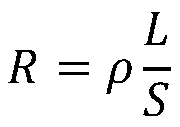
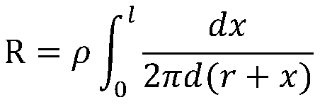
Especially below the scale of 10nm, the resistance value of the amorphous phase becomes very large, resulting in the reading current being too small to read correctly, requiring a larger current to read; while the resistance value of the crystalline phase is very small, and it is easy to read with a large current. Tunneling shows the characteristics of a short-circuit circuit, and the difference between the resistance value of the amorphous state is too large, and it cannot be read within the range of the same test instrument
[0005] Therefore, it is necessary to propose a new electrode configuration structure suitable for nanoscale phase change units to solve the problem of large differences in resistance between the two phases.

Method used


Image

  • Novel electrode configuration structure used for nanometer-level phase change memory unit
  • Novel electrode configuration structure used for nanometer-level phase change memory unit
  • Novel electrode configuration structure used for nanometer-level phase change memory unit

Examples


Embodiment Construction

[0031] In order to make the object, technical solution and advantages of the present invention clearer, the present invention will be further described in detail below in conjunction with the accompanying drawings and embodiments. It should be understood that the specific embodiments described here are only used to explain the present invention, not to limit the present invention. In addition, the technical features involved in the various embodiments of the present invention described below can be combined with each other as long as they do not constitute a conflict with each other. The present invention will be further described in detail below in combination with specific embodiments.

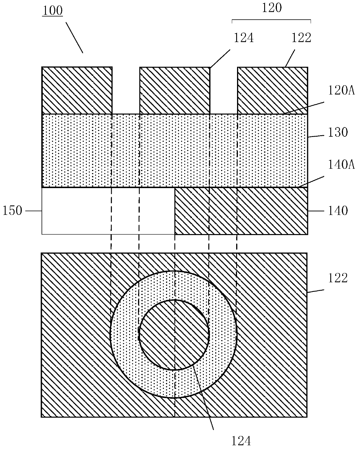
[0032] As a preferred embodiment of the present invention, such as figure 1 As shown, the present invention provides a novel electrode configuration structure for nanoscale phase change memory cells, wherein:

[0033] The novel electrode configuration structure 100 includes an upper electr...


PUM


Abstract

The invention discloses a novel electrode configuration structure used for a nanometer-level phase change memory unit. The new electrode configuration includes an upper-layer electrode material layer,an intermediate phase change material layer and a lower-layer electrode material layer. The upper-layer electrode material layer includes an outer ring electrode and an internal source end electrode.The upper-layer electrode material layer and the internal source end electrode are an asymmetric upper and lower electrode structure, and horizontal projection has an intersection relationship. Two electrode configuration manners are constructed at the same time in the same unit, a horizontal working mode is adopted in a high-resistance non-crystallization process, an equivalent resistance R is significantly reduced, a read current is increased, and correct reading is facilitated; a vertical working mode is adopted in a low-resistance crystallization process, the equivalent resistance R is increased, a working current is reduced, tunneling of a large current is avoided, and device life is extended; and thus disparity of two phase resistances of nanometer-level phase change material is reduced, and external access circuits are simplified and unified.

Description

technical field [0001] The invention belongs to the field of microelectronics and relates to a novel electrode configuration structure for a nanoscale phase-change memory unit, in particular to the design and application of a phase-change memory element based on a chalcogenide phase-change material. Background technique [0002] The phase change memory based on the chalcogenide phase change material can store information and data through the huge resistance difference between the crystalline phase and the amorphous phase, and can even achieve multi-level phase change storage. This phase-change process has the advantages of low power consumption and high-density cost as the size decreases, so the industry pays great attention to the development of nanoscale phase-change memory. [0003] At present, there are relatively mature applications in the structural design of phase change units, such as T-shaped structure and side wall contact structure, etc. The purpose is to reduce t...

Claims


Application Information

Patent Timeline
Patent Type & Authority Applications(China)
IPC IPC(8): H01L45/00
CPCH10N70/841H10N70/231
Inventor 马平童浩缪向水
Owner HUAZHONG UNIV OF SCI & TECH
Why Eureka
Try Eureka