


Quick Research
Generate reliable direction feasibility study reports for your R&D in just a few steps.

Technical Q&A
Discover and master advanced knowledge NOW. Basics, ideas, possibilities, all at once.

Find Solutions
As an expert in R&D theories, this can generate solutions to your technical problems instantly.

Evaluate Feasibility
Analyze your overall solution with one click, know your potential R&D risks in advance.

Monitor Landscape
Get weekly tech updates, stay abreast of the latest tech innovations and key insights.
Plasma treatment apparatus
A processing device and plasma technology, applied in the directions of plasma, discharge tubes, electrical components, etc., can solve the problems of damage to the yield of semiconductor devices and increase of circuit performance, so as to suppress the unevenness of the electric field, reduce the deviation of processing, The effect of improving the yield
- Summary
- Abstract
- Description
- Claims
- Application Information
AI Technical Summary
Problems solved by technology
Method used
Image


Examples
Embodiment Construction
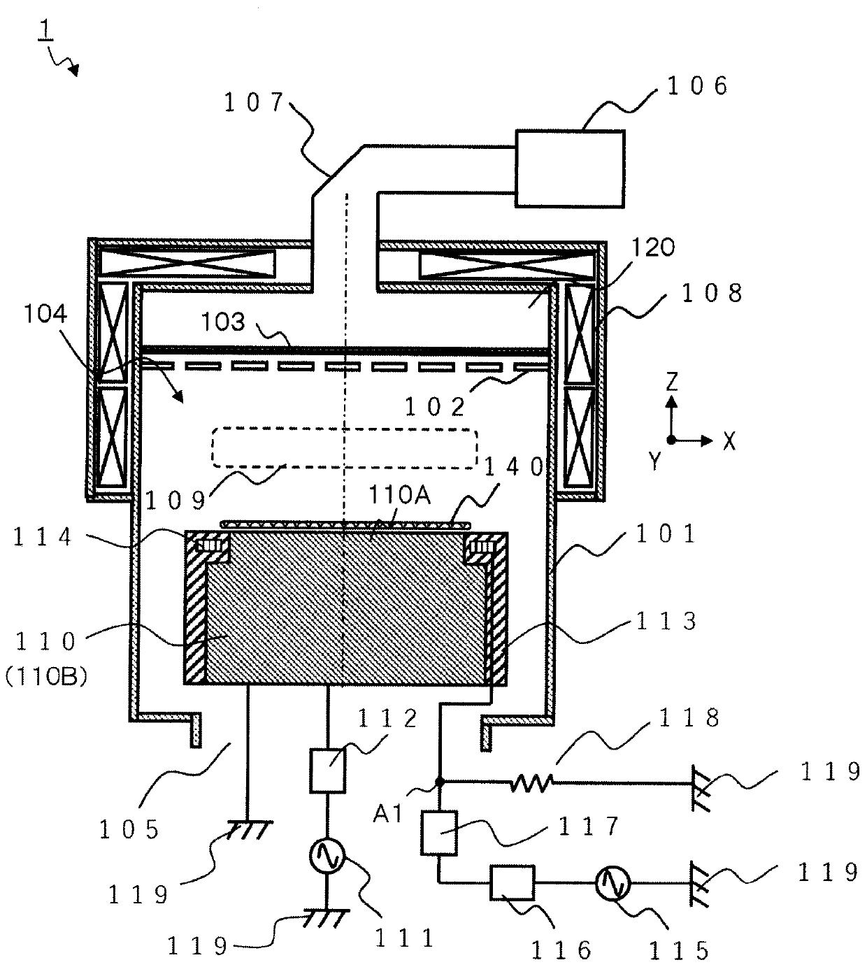
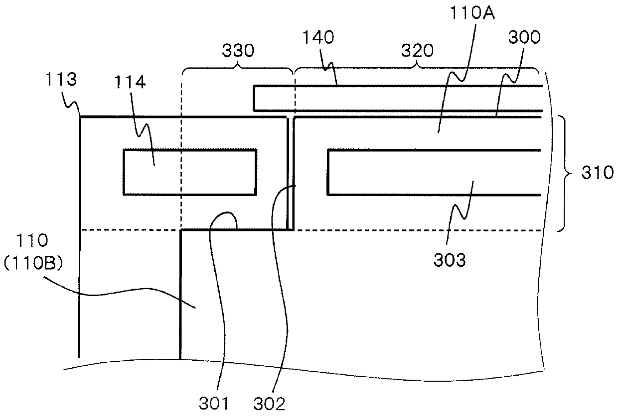
[0022] Below, use Figure 1 ~ Figure 3 A plasma processing apparatus according to one embodiment of the present invention will be described.
[0023] [Plasma treatment device (1)]
[0024] figure 1 It is a vertical cross-sectional view schematically showing the outline of the structure of the plasma processing apparatus 1 according to one embodiment of the present invention. In addition, the X direction, the Y direction, and the Z direction are used for description. The Z direction is a vertical direction and is a direction of a central axis of a shape such as a cylinder. The X direction and the Y direction are two directions constituting a horizontal plane perpendicular to the Z direction, a surface such as a wafer, and correspond to radial directions. exist figure 1 , shows a cross section centered on the central axis of the dot-dash line in the Z direction.
[0025] In the plasma processing apparatus 1 of the present embodiment, a configuration example related to a mi...
PUM
 Abstract
Description
Claims
Application Information
 - R&D Engineer
- R&D Manager
- IP Professional
- Industry Leading Data Capabilities
- Powerful AI technology
- Patent DNA Extraction
Browse by: Latest US Patents, China's latest patents, Technical Efficacy Thesaurus, Application Domain, Technology Topic, Popular Technical Reports.
© 2024 PatSnap. All rights reserved.Legal|Privacy policy|Modern Slavery Act Transparency Statement|Sitemap|About US| Contact US: help@patsnap.com