A kind of recycling and processing equipment for microelectronic materials and semiconductor raw materials

A processing equipment and semiconductor technology, applied in lighting and heating equipment, drying gas layout, solid waste removal, etc., can solve the problems of multiple operators, inability to adjust production speed, production line length, etc., to improve crushing efficiency and reduce occupation. Effects of space and labor costs

Active Publication Date: 2021-07-23
湖州力卓机械设备技术开发有限公司
View PDF9 Cites 0 Cited by
  • Summary
  • Abstract
  • Description
  • Claims
  • Application Information

AI Technical Summary

Problems solved by technology

[0004] To sum up, the semiconductor raw material recovery and reuse equipment in the prior art has the following disadvantages: first, there are many production processes, the production line is long, and it needs to occupy more production space and be equipped with more operators; 2. Raw materials are easy to accumulate somewhere on the upper end of the crushing roller during crushing, resulting in a significant reduction in crushing efficiency; 3. The production speed between various processes cannot be automatically adjusted, and manual adjustment is required, which not only troubles the operation, but also increases labor intensity. , and the operation process is prone to errors, leading to chaos in production

Method used


Image

  • A kind of recycling and processing equipment for microelectronic materials and semiconductor raw materials
  • A kind of recycling and processing equipment for microelectronic materials and semiconductor raw materials

Examples


Embodiment Construction

[0020] The following will clearly and completely describe the technical solutions in the embodiments of the present invention with reference to the accompanying drawings in the embodiments of the present invention. Obviously, the described embodiments are only some, not all, embodiments of the present invention.

[0021] In describing the present invention, it should be understood that the terms "upper", "lower", "front", "rear", "left", "right", "top", "bottom", "inner", " The orientation or positional relationship indicated by "outside", etc. is based on the orientation or positional relationship shown in the drawings, and is only for the convenience of describing the present invention and simplifying the description, rather than indicating or implying that the referred device or element must have a specific orientation, so as to Specific orientation configurations and operations, therefore, are not to be construed as limitations on the invention.

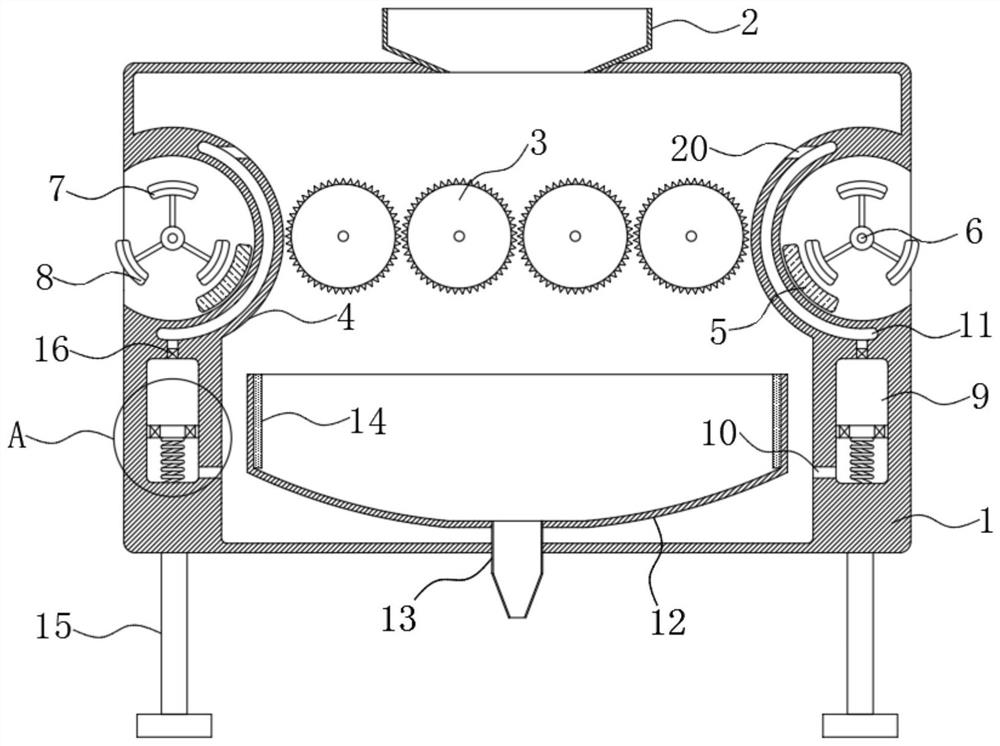
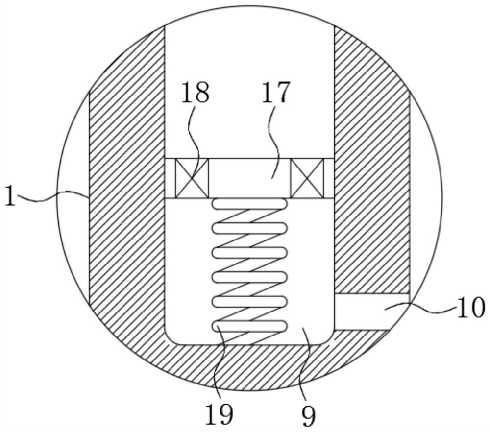
[0022] refer to Figure ...


PUM


Abstract

The invention discloses a device for recycling and processing microelectronic materials and semiconductor raw materials, which comprises a box body and a melting box arranged inside the box body. There are outriggers, an electric heating plate is fixedly installed on the inner wall of the melting box, a discharge nozzle connected with the outside of the box is provided at the lower end of the melting box, and a plurality of crushing rollers are evenly distributed on the upper end of the inner wall of the box. The invention integrates the drying, crushing and melting processes in the recycling process of semiconductor raw materials by setting the driving mechanism, crushing roller, electric heating plate, pumping mechanism, air guide chamber and gas injection port, reducing the space occupied by the production line and Labor costs can also be blown and spread the raw materials on the crushing roller to improve the crushing efficiency. At the same time, it can automatically realize the positive correlation adjustment of the production speed between each process, without manual operation, reduce labor intensity, and is not easy to make mistakes, avoiding production Into chaos.

Description

technical field [0001] The invention relates to the technical field of semiconductor reprocessing equipment, in particular to a recycling and processing equipment for microelectronic materials and semiconductor raw materials. Background technique [0002] Microelectronic material is a kind of semiconductor material synthesized by GeSi alloy and wide bandgap. Microelectronic material and devices are the foundation of microelectronic industry. In order to promote the development of microelectronic industry and make full use of materials, the general Waste microelectronic materials and semiconductor raw materials will be recycled and reprocessed for secondary use. [0003] The existing recycling and reprocessing process of semiconductor raw materials generally includes cleaning, drying, crushing, melting and recasting of raw materials, which leads to a long production line for recycling and reprocessing semiconductor raw materials, and each process on the production line needs ...

Claims


Application Information

Patent Timeline
Patent Type & Authority Patents(China)
IPC IPC(8): B02C4/08B02C4/30B02C4/42B02C4/28B09B3/00F26B21/00
CPCB02C4/08B02C4/30B02C4/42B02C4/28F26B21/001B02C2201/06B09B3/40
Inventor 曹明丽
Owner 湖州力卓机械设备技术开发有限公司
Why Eureka
Try Eureka