Novel method for correcting OPC model

A correction method and model technology, which is applied in the photoengraving process of the pattern surface, the original for opto-mechanical processing, optics, etc., can solve the problem of increasing the accuracy of the feedback data, the deviation between the data and the actual value, and the time-consuming, etc. problems, to achieve the effect of improving speed and peak yield, improving chip performance and yield, and reducing the number of iterations

Pending Publication Date: 2020-02-11
UNITED MICROELECTRONICS CENT CO LTD
View PDF2 Cites 4 Cited by
  • Summary
  • Abstract
  • Description
  • Claims
  • Application Information

AI Technical Summary

Problems solved by technology

However, due to the large amount of measured data and time-consuming, the graphics under the Non-Manhattans design rules are not easy to describe. It is difficult to characterize and describe the actual graphics through the measurement data of several points. The photoresist will shrink under the bombard

Method used


Image

  • Novel method for correcting OPC model

Examples


Embodiment Construction

[0021] The technical solutions in the present invention will be further described below in conjunction with the accompanying drawings and embodiments.

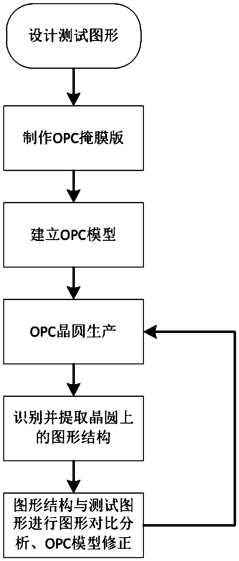
[0022] Such as figure 1 As shown, a calibration method for a new OPC model includes the following steps:

[0023] A correction method for a novel OPC model, comprising the following steps:

[0024] A. Design OPC test pattern;

[0025] B. Make OPC mask plate;

[0026] C. Establish OPC model;

[0027] D. Carry out OPC wafer production to manufacture a physical structure corresponding to the test pattern on the wafer; the physical structure may include electronic devices or semiconductor devices, connecting wires, signs, and the like.

[0028] E, identifying and extracting the graphic structure on the wafer produced in step D;

[0029] F, compare and analyze the graphic structure extracted on the wafer in step E and the test pattern designed in step A, so as to obtain the mismatching or wrong part of the graphic structure on...


PUM


Abstract

The invention proposes a novel method for correcting an OPC model, which includes the following steps: designing an OPC test pattern; making an OPC mask plate for the OPC test pattern; establishing anOPC model; producing an OPC wafer; identifying and extracting a pattern structure from the produced wafer; comparing the pattern structure extracted from the wafer with the designed test pattern to obtain the unmatched or incorrect part of the pattern structure on the wafer relative to the test pattern; correcting the OPC model based on the part not matching the test pattern determined in the pattern comparative analysis; repeating the iteration until the pattern structure of the wafer completely matches the test pattern or satisfies a design accuracy requirement in the pattern comparative analysis such that the OPC model correction is completed. The method avoids the potential risk caused by replacing the photoresist, accurately acquires and feeds back the information of complex patterns, and greatly reduces the number of iterations in the model design-modification-model determination process.

Description

technical field [0001] The invention relates to the field of semiconductor design and manufacture, in particular to a correction method for a novel OPC model. Background technique [0002] The key to model-based optical proximity effect correction is to establish an accurate photolithography process model. A reliable OPC model can fully describe the entire photolithography process including optical system, mask, photoresist, and etching process. Although the strict lithography model has high precision, it also requires high computing power. The existing computing power cannot complete the chip-level lithography process simulation within the time required by the market. Therefore, OPC uses a semi-empirical simplified lithography model, which replaces the complex process in the original model with some simplified empirical formulas. The empirical formula contains many parameters, which can be calibrated by fitting the experimental data, and finally make the calculation struc...

Claims


Application Information

Patent Timeline
IPC IPC(8): G03F1/36G03F7/20
CPCG03F1/36G03F7/70441
Inventor 陈世杰郭进王学毅刘荣侃
Owner UNITED MICROELECTRONICS CENT CO LTD
Why Eureka
Try Eureka