A method for preparing a high-reliability photovoltaic inverter printed circuit board

A technology for photovoltaic inverters and printed circuit boards, which is applied in the fields of printed circuit manufacturing, printed circuit, and multilayer circuit manufacturing, and can solve the problems of high layers and thick boards of photovoltaic inverters

Active Publication Date: 2020-07-07
惠州市大亚湾科翔科技电路板有限公司
View PDF17 Cites 0 Cited by
  • Summary
  • Abstract
  • Description
  • Claims
  • Application Information

AI Technical Summary

Problems solved by technology

[0005] In order to solve the above technical problems, the present invention proposes a method for preparing a high-reliability photovoltaic inverter printed circuit board, which aims to solve various defects caused by the high number of layers and thick board thickness of the existing photovoltaic inverter question

Method used


Image

  • A method for preparing a high-reliability photovoltaic inverter printed circuit board
  • A method for preparing a high-reliability photovoltaic inverter printed circuit board

Examples


Embodiment Construction

[0028] The present invention will be further described below in conjunction with the accompanying drawings and embodiments.

[0029] In order to enable those skilled in the art to better understand the solutions of the present invention, the following will clearly and completely describe the technical solutions in the embodiments of the present invention in conjunction with the drawings in the embodiments of the present invention. Obviously, the described embodiments are only It is a part of embodiments of the present invention, but not all embodiments. Based on the embodiments of the present invention, all other embodiments obtained by persons of ordinary skill in the art without making creative efforts belong to the protection scope of the present invention.

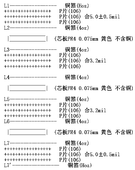
[0030] The invention provides a method for preparing a high-reliability photovoltaic inverter printed circuit board. Specifically, the process includes the following steps.

[0031] Cutting and baking board, inner lay...


PUM


Abstract

The invention provides a preparation method of a high-reliability printed circuit board of photovoltaic inverters, and specifically relates to a preparation method of multi-layer board. After the L1 to L7 layers and the L8 to L14 layers are respectively processed and prepared, the L1 to L14 layers are laminated. In the process, a different hole copper manufacturing process, a high multi-layer lamination manufacturing process and a depth control drilling depth control process are further designed for processing control and manufacturing. The problem of various defects in the production of existing multi-layer laminated circuit boards is solved, the production cost of the circuit board is greatly reduced, and the quality and production efficiency of the high-thickness multilayer circuit board are improved.

Description

technical field [0001] The invention relates to a manufacturing process of a copper plate, in particular to a method for preparing a printed circuit board of a high-reliability photovoltaic inverter. Background technique [0002] Photovoltaic inverter is a power adjustment device composed of semiconductor devices. It is mainly used to convert DC power into AC power. It is generally composed of a boost circuit and an inverter bridge circuit. The boost circuit boosts the DC voltage of the solar battery to the DC voltage required for inverter output control; the inverter bridge circuit converts the boosted DC voltage into an AC voltage of common frequency equivalently. [0003] Photovoltaic inverter printed circuit board (Printed Circuit Board, PCB) is an important part of the photovoltaic inverter, which undertakes the important function of current transmission. During long-term use, its heat generation is very large. , the signal control is precise, and the surface copper an...

Claims


Application Information

Patent Timeline
Patent Type & Authority Patents(China)
IPC IPC(8): H05K3/46H05K3/42H05K3/00
CPCH05K3/0047H05K3/429H05K3/4611
Inventor 周刚王欣曾祥福
Owner 惠州市大亚湾科翔科技电路板有限公司
Why Eureka
Try Eureka