Ultraviolet LED packaging structure

A technology of LED packaging and ultraviolet light, applied in electrical components, circuits, semiconductor devices, etc., can solve the problems of high cost and complex process of ultraviolet light emitting diodes

Inactive Publication Date: 2020-02-18
SHENZHEN ROUSHENG TECH CO LTD +1
View PDF5 Cites 0 Cited by
  • Summary
  • Abstract
  • Description
  • Claims
  • Application Information

AI Technical Summary

Problems solved by technology

The above-mentioned ultraviolet light-emitting diode and packaging method are complicated in technology and high in cost

Method used


Image

  • Ultraviolet LED packaging structure
  • Ultraviolet LED packaging structure
  • Ultraviolet LED packaging structure

Examples


Embodiment Construction

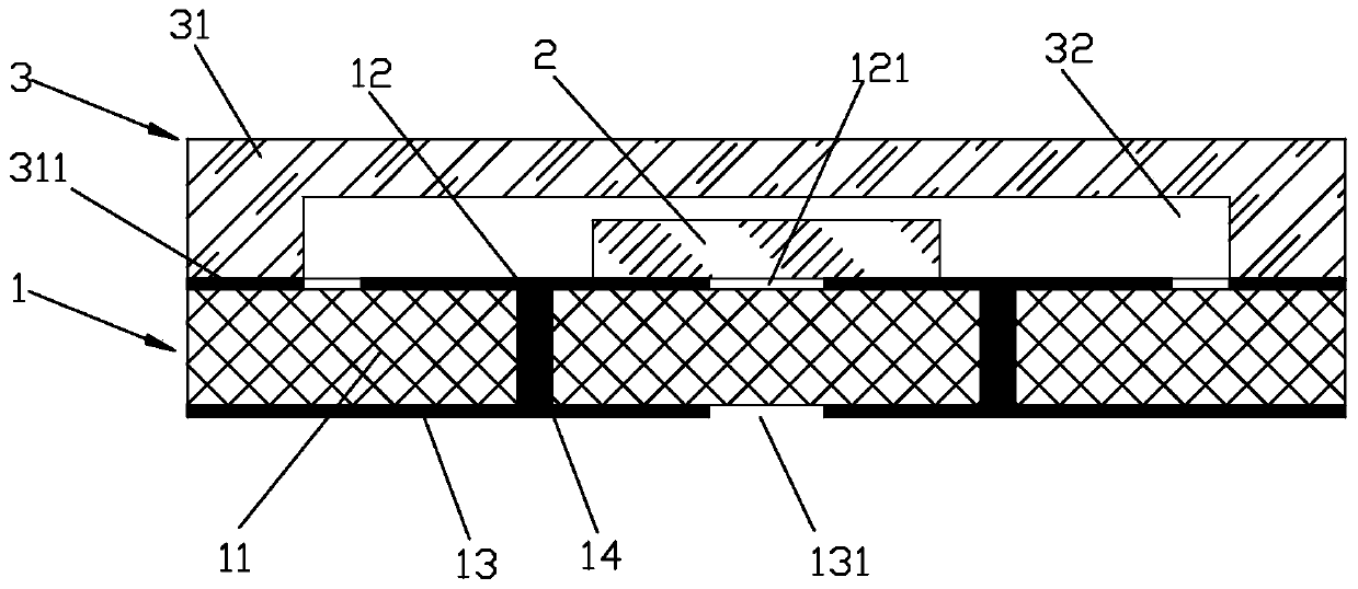
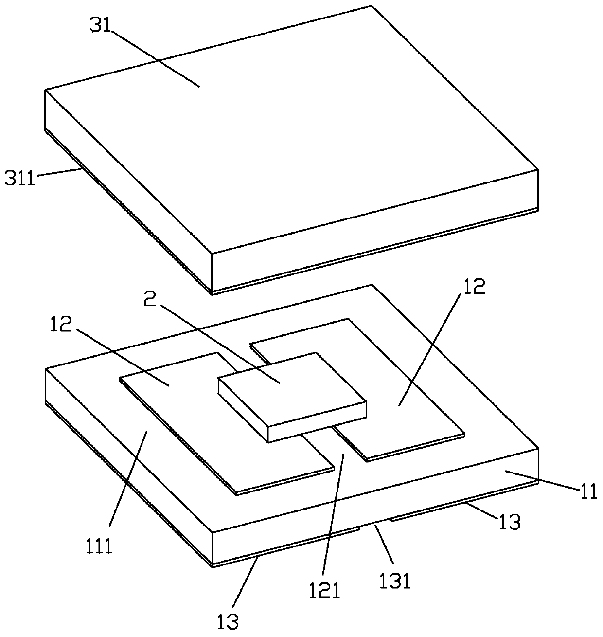
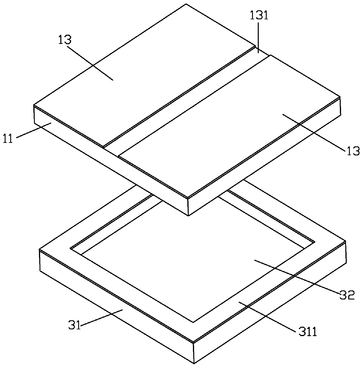
[0025] Please check Figure 1 to Figure 3 , UV LED packaging structure, including base 1, UV LED chip 2 and window 3.

[0026] The base 1 includes a substrate 11, such as a silicon-based material or a ceramic material, the top surface of the substrate 11 is provided with a top metal layer 12, the bottom surface of the substrate 11 is provided with a bottom metal layer 13, and the substrate 11 is provided with a through hole penetrating the top and bottom, and a conductive body 14 is additionally provided. The conductive body 14 is located in the through hole. The conductive body 14 is fixed and electrically connected to the top and bottom metal layers 12 and 13 to form a whole. In this embodiment: the top surface of the substrate 11 is provided with two top metal layers 12 spaced apart, an upper space 121 is formed between the two top metal layers 12, and the top surface of the substrate 11 is The Japanese-shaped area covered by the metal layer 12 (the two top metal layers 12 ar...


PUM

PropertyMeasurementUnit
glass transition temperatureaaaaaaaaaa

Abstract

The invention discloses an ultraviolet LED packaging structure which comprises a base, an ultraviolet LED chip and a window piece. The base comprises a substrate. The top and bottom surfaces of the substrate are respectively provided with top and bottom metal layers. The substrate is provided with through holes penetrating through the top and the bottom. An electrical conductor is additionally arranged. The electrical conductor is located in the through holes, and the electrical conductor is fixedly connected and electrically connected with the top and bottom metal layers to form a whole. Theultraviolet LED chip is installed on the top surface of the base and electrically connected with the top metal layer. The window piece comprises quartz glass. The bottom surface of the quartz glass isconcavely provided with a concave cavity. The bottom surface of the quartz glass is adhered to the top surface of the base through an inorganic adhesive, and the concave cavity is connected with theultraviolet LED chip in a covering way. The ultraviolet LED packaging structure has the following advantages: simple process, low packaging cost, airtight packaging and inorganic packaging.

Description

Technical field [0001] The invention relates to an LED packaging structure, in particular to an ultraviolet LED packaging structure. Background technique [0002] Existing UV LEDs and packaging methods, such as CN108231976A. The ultraviolet light emitting diode includes: a quartz glass cover plate, a substrate, an ultraviolet light emitting diode chip, a first metal layer, a solder layer, a second metal layer, and a circuit structure layer; the substrate is provided with a groove, and the quartz glass cover plate covers the substrate On the groove, the shape of the groove is set corresponding to the shape of the quartz glass cover, the top surface of the substrate is provided with the second metal layer; the surface of the quartz glass cover in contact with the groove is provided with the first metal layer; solder The layer is arranged between the second metal layer and the first metal layer, and the solder layer is used to weld the second metal layer and the first metal layer t...

Claims


Application Information

Patent Timeline
Patent Type & Authority Applications(China)
IPC IPC(8): H01L33/48H01L33/56H01L33/60H01L33/62
CPCH01L33/48H01L33/56H01L33/60H01L33/62
Inventor 刘忠吴启保
Owner SHENZHEN ROUSHENG TECH CO LTD
Why Eureka
Try Eureka