
Programming method and system of memory

A programming method and memory technology, which are applied in the memory programming method and system field, can solve the problems of high power consumption of the memory, and achieve the effects of saving energy, reducing power consumption, and reducing power consumption

Inactive Publication Date: 2020-02-25
GIGADEVICE SEMICON (BEIJING) INC
View PDF10 Cites 0 Cited by
  • Summary
  • Abstract
  • Description
  • Claims
  • Application Information

AI Technical Summary

Problems solved by technology

[0004] The invention provides a memory programming method and system to solve the technical problem of high power consumption during memory programming

Method used


Image

  • Programming method and system of memory
  • Programming method and system of memory
  • Programming method and system of memory

Examples


Embodiment A

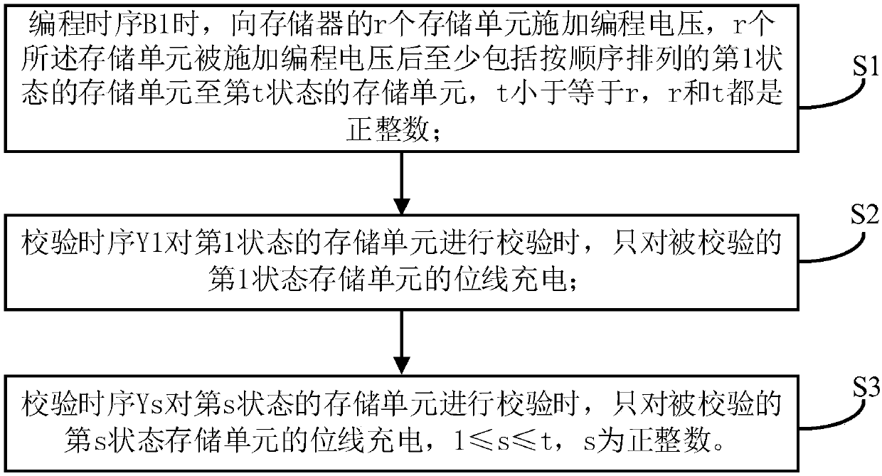
[0025] see figure 1 , figure 1 It is a schematic flow chart of a memory programming method in Embodiment A of the present invention. The memory programming method is used to improve the durability and ease of use of data read from the memory, so as to improve the life of the memory. The memory programming method includes the following steps:

[0026] Step S1: In programming sequence B1, apply a programming voltage to r storage cells of the memory, and the r storage cells include at least the storage cells in the first state to the storage cells in the t-th state arranged in order after the programming voltage is applied, t is less than or equal to r, r and t are both positive integers;

[0027] Step S2: When the verification sequence Y1 verifies the memory cells in the first state, only charge the bit lines of the memory cells in the first state to be verified;

[0028] Step S3: When verifying the memory cell in the sth state in the verification sequence Ys, only charge the ...

Embodiment B

[0041] see Figure 6 , Figure 6 It is a schematic diagram of the module structure of the programming system 12 of the memory of the present invention. The memory programming system 12 can execute the memory programming method provided by any embodiment of the present invention. The memory programming system 12 includes:

[0042] The programming module 121 is used to apply a programming voltage to the r storage cells of the memory when the programming sequence B1 is used. After the r storage cells are applied with the programming voltage, at least the storage cells in the first state to the t state are arranged in order. Storage unit, t is less than or equal to r, r and t are both positive integers;

[0043] The verification module 122 is used to verify the memory cell in the first state when the verification sequence Y1 is used to only charge the bit line of the verified first state memory cell; the verification sequence Ys is for the memory cell in the s state When perfo...


PUM


Abstract

The invention discloses a programming method and system of a memory. The programming method of the memory comprises the following steps that when a time sequence B1 is programmed, programming voltageis applied to r storage units of the memory, wherein the r storage units at least comprise storage units in a first state and storage units in a t-th state which are arranged in sequence after the programming voltage is applied, t is smaller than or equal to r, and r and t are both positive integers; when the storage units in the first state are verified by the verification time sequence Y1, onlybit lines of the verified storage units in the first state are charged; and when the storage unit in the s-th state is verified by the verification time sequence Ys, only the bit line of the verified storage unit in the s-th state is charged, s is greater than or equal to 1 and less than or equal to t, and s is a positive integer. The programming method and system of the memory have the advantage of saving power consumption.

Description

technical field [0001] The embodiments of the present invention relate to the technical field of memory, and in particular, to a memory programming method and system. Background technique [0002] Memory is a component that must be used in programming, such as Nand flash memory. Nand flash memory is a kind of non-volatile memory, which has the advantages of fast rewriting speed and large storage capacity. In the Nand flash memory, especially the TLC type memory, the state of the storage unit is more, and when performing programming verification, more electric energy is needed and the power consumption is larger. [0003] Therefore, how to reduce the power consumption of storage has become a demand in the field of memory technology. Contents of the invention [0004] The invention provides a memory programming method and system to solve the technical problem of high power consumption during memory programming. [0005] In a first aspect, an embodiment of the present inven...

Claims


Application Information

Patent Timeline
IPC IPC(8): G11C16/10G11C16/34
CPCG11C16/10G11C16/3404
Inventor 贺元魁潘荣华
Owner GIGADEVICE SEMICON (BEIJING) INC
Learn More