Wafer slicing method and chip

A wafer and slicing technology, applied in the manufacture of electrical components, electrical solid devices, semiconductor/solid devices, etc., can solve problems such as edge cracking and missing corners, and achieve the effect of increasing the number of survivors and chip production

Pending Publication Date: 2020-02-25
WILL SEMICON (SHANGHAI) CO LTD
View PDF4 Cites 4 Cited by
  • Summary
  • Abstract
  • Description
  • Claims
  • Application Information

AI Technical Summary

Problems solved by technology

[0004] The purpose of the embodiments of the present invention can solve the problem of edge cracking and missing corners caused by dicing in the prior art for dividing wafers

Method used


Image

  • Wafer slicing method and chip
  • Wafer slicing method and chip
  • Wafer slicing method and chip

Examples


Embodiment Construction

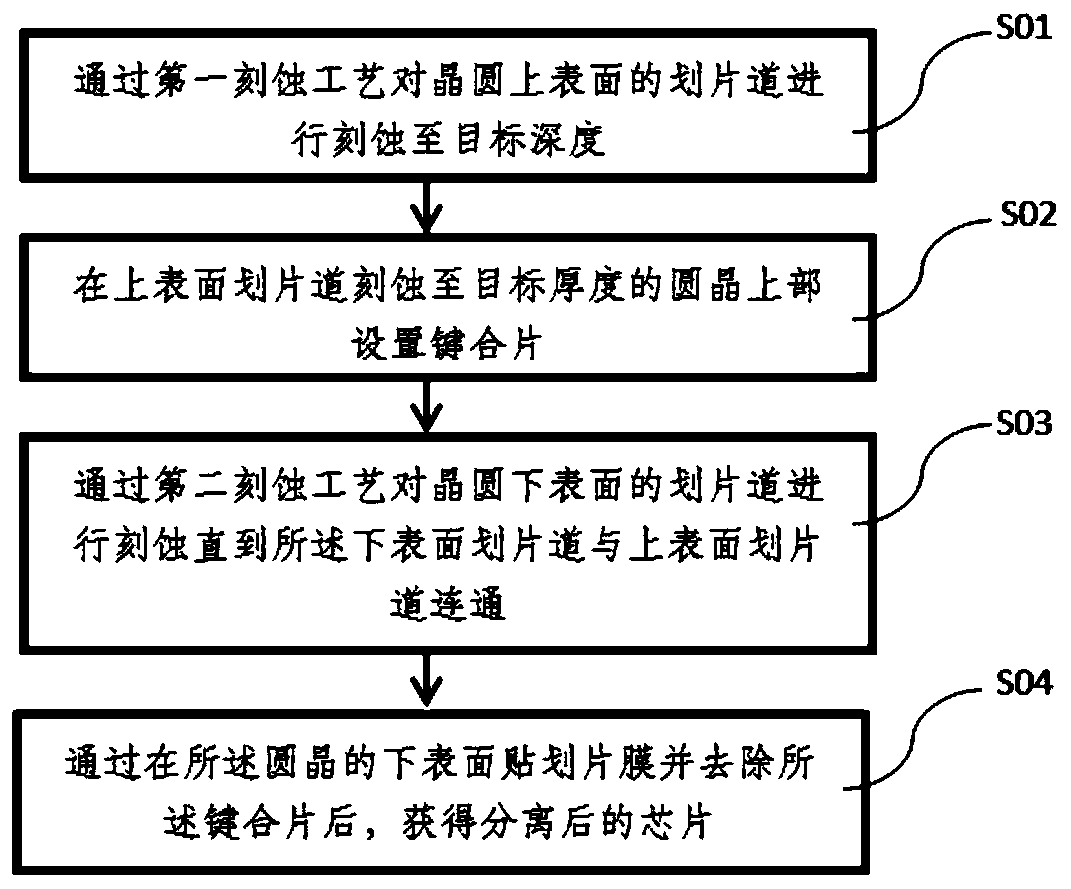
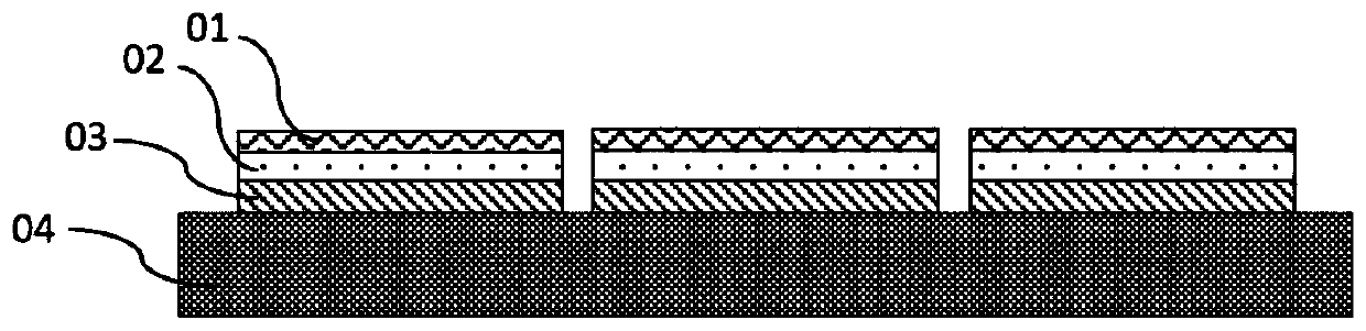
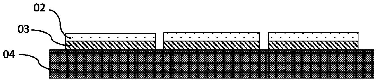
[0028] In order to make the purpose, technical solutions and advantages of the embodiments of the present invention clearer, the technical solutions in the embodiments of the present invention will be clearly and completely described below in conjunction with the drawings in the embodiments of the present invention. Obviously, the described embodiments It is a part of embodiments of the present invention, but not all embodiments. Based on the embodiments of the present invention, all other embodiments obtained by persons of ordinary skill in the art without creative efforts fall within the protection scope of the present invention.

[0029] It should be noted that the terms "first" and "second" in the description and claims of the present invention and the above drawings are used to distinguish similar objects, but not necessarily used to describe a specific sequence or sequence. It is to be understood that the data so used are interchangeable under appropriate circumstances s...


PUM


Abstract

The invention discloses a wafer slicing method. The method comprises the following steps of: etching a scribing channel on the upper surface of a wafer to a target depth through a first etching process, arranging a bonding sheet at the upper part of the wafer of which the upper surface scribing channel is etched to the target thickness, etching the scribing channel on the lower surface of the wafer through a second etching process until the scribing channel on the lower surface is communicated with the scribing channel on the upper surface, and pasting a scribing film on the lower surface of the wafer and removing the bonding sheet to obtain a separated chip. The invention further discloses a chip manufactured through the slicing method. According to the technical scheme, the survival number of the chips on each wafer is greatly increased, and the yield of the chips is greatly increased.

Description

technical field [0001] The invention relates to the technical field of semiconductor manufacturing, in particular to a wafer slicing method and a chip. Background technique [0002] The current wafer slicing process is to cut the silicon wafer into individual chips by a dicing machine, and then take out the chip with a chip picking device or manually. [0003] However, the diamond knife used to split the wafer will cause the edge of the chip to crack, and the corner will be chipped, which will seriously damage the chip structure, resulting in electrical failure and loss of yield. In addition, tiny silicon cracks will extend and spread, which will greatly affect the subsequent reliability and service life. As the size of semiconductor devices gradually decreases, the usual 60um dicing lanes have greatly affected the number of chips. However, because blade scribing is a mechanical form, it is mainly limited by the width of the blade body, which is an insurmountable technolog...

Claims


Application Information

Patent Timeline
Patent Type & Authority Applications(China)
IPC IPC(8): H01L21/306H01L21/308H01L21/683H01L21/78
CPCH01L21/30604H01L21/308H01L21/6835H01L21/78H01L2221/68327
Inventor 诸舜杰阮孟波董建新
Owner WILL SEMICON (SHANGHAI) CO LTD
Why Eureka
Try Eureka