On-chip monitoring circuit of anti-fuse FPGA

A monitoring circuit and anti-fuse technology, applied in hardware monitoring, electrical digital data processing, error detection/correction, etc., can solve problems such as difficulty in accurately monitoring signal transmission speed

Active Publication Date: 2020-02-28
58TH RES INST OF CETC
View PDF7 Cites 3 Cited by
  • Summary
  • Abstract
  • Description
  • Claims
  • Application Information

AI Technical Summary

Problems solved by technology

[0005] The object of the present invention is to provide a kind of on-chip monitoring circuit of antifuse FPGA, to solve the problem that it is difficult to accurately monitor the transmission speed of signals after each antifuse FPGA programming

Method used


Image

  • On-chip monitoring circuit of anti-fuse FPGA
  • On-chip monitoring circuit of anti-fuse FPGA

Examples


Embodiment 1

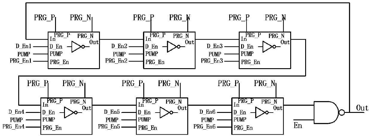
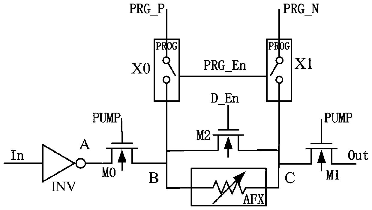
[0032] The invention provides an on-chip monitoring circuit of an antifuse FPGA, its structure is as follows: figure 1 As shown, it includes an even-numbered delay unit circuit and a NAND gate circuit; in the first embodiment, the number of the delay unit circuits is 6, and the output terminal of a delay unit circuit is connected to the next delay unit circuit. The input end of the time unit circuit, 6 described delay unit circuits are connected in series to an input end of the NAND gate circuit; the other input end of the NAND gate circuit is connected to the monitoring enable signal En; The output end of the NAND gate circuit is connected to the input end of the first delay unit circuit to form a ring circuit. When the monitoring enable signal En was low, the on-chip monitoring circuit of the antifuse FPGA output a fixed high level and stopped working; when the monitoring enabling signal En was high, the on-chip monitoring circuit of the antifuse FPGA start working. Specif...


PUM


Abstract

The invention discloses an on-chip monitoring circuit of an anti-fuse FPGA,and belongs to the technical field of semiconductor integrated circuits. The on-chip monitoring circuit of the anti-fuse FPGAcomprises an even number of stages of delay unit circuits and an NAND gate circuit,the delay unit circuits are connected in series and then connected to one input end of the NAND gate circuit; a monitoring enable signal En is accessed to the other input end of the NAND gate circuit; and the output end of the NAND gate circuit is connected with the input end of the first delay unit circuit to forma loop circuit. After the anti-fuse FPGA chip is manufactured,the anti-fuse units in the delay unit circuit are programmed,and signals are enabled to pass through different numbers of anti-fuse unitsrespectively,so that the speed performance of the signals after the anti-fuse FPGA is programmed and configured by a user and transmitted to pass through different numbers of anti-fuse units under different conditions is evaluated.

Description

technical field [0001] The invention relates to the technical field of semiconductor integrated circuits, in particular to an on-chip monitoring circuit of an antifuse FPGA. Background technique [0002] In electronic systems, FPGAs can flexibly implement various user-customized functions according to user configurations, thus being widely used. According to different programming logic structures, FPGAs can be divided into SRAM-based FPGAs, anti-fuse unit-based FPGAs, and Flash-based FPGAs. Since the antifuse unit occupies a small layout area, the wiring resources of the antifuse FPGA are much richer than that of the SRAM FPGA under the same scale. After the anti-fuse FPGA is programmed, the program will not be lost after power failure, and there is no need to reload the programming configuration information when power is turned on. It is easy to use and has good security and confidentiality. At the same time, the anti-fuse unit structure naturally has good radiation resis...

Claims


Application Information

Patent Timeline
Patent Type & Authority Applications(China)
IPC IPC(8): G06F11/30G11C17/16
CPCG06F11/3037G06F11/3055G11C17/165
Inventor 王文曹靓赵桂林
Owner 58TH RES INST OF CETC
Why Eureka
Try Eureka