
Shallow trench isolation structure and forming method thereof, and semiconductor device and forming method thereof

An isolation structure and shallow trench technology, applied in semiconductor/solid-state device manufacturing, electrical components, circuits, etc., can solve problems such as reducing device reliability, and achieve the effects of improving reliability, reducing hammer effect, and reducing interaction.

Pending Publication Date: 2020-03-10
CHANGXIN MEMORY TECH INC
View PDF0 Cites 3 Cited by
  • Summary
  • Abstract
  • Description
  • Claims
  • Application Information

AI Technical Summary

Problems solved by technology

As the integration level increases, adjacent MOSFETs will affect each other. For example, when a MOSFET is turned on and off, it will affect its adjacent MOSFET due to the capacitive coupling effect. This effect is called the hammer effect. (HammerEffect), thereby reducing the reliability of the device

Method used


Image

  • Shallow trench isolation structure and forming method thereof, and semiconductor device and forming method thereof
  • Shallow trench isolation structure and forming method thereof, and semiconductor device and forming method thereof
  • Shallow trench isolation structure and forming method thereof, and semiconductor device and forming method thereof

Examples


Embodiment Construction

[0054] The specific implementation manner of the present invention will be described in more detail below with reference to schematic diagrams. The advantages and features of the present invention will be more apparent from the following description. It should be noted that all the drawings are in a very simplified form and use imprecise scales, and are only used to facilitate and clearly assist the purpose of illustrating the embodiments of the present invention.

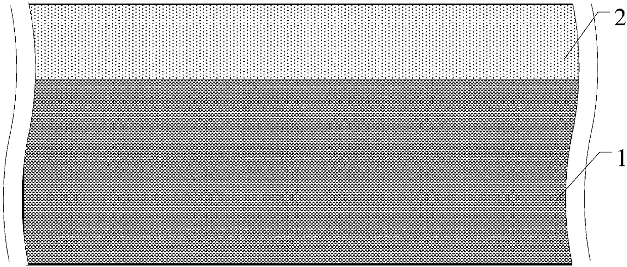
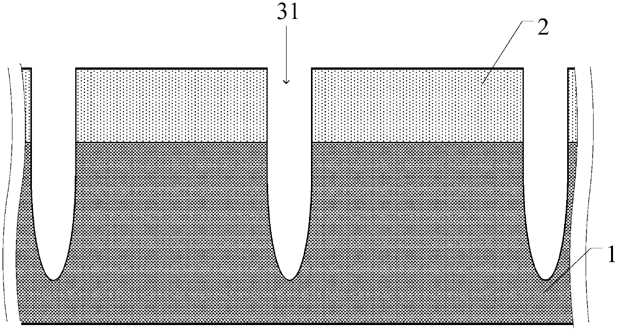
[0055] please participate Figure 7 or Figure 11 , the present embodiment provides a shallow trench isolation structure, the shallow trench isolation structure is formed in a substrate 1 and defines a plurality of active regions 2, and the shallow trench isolation structure is formed with several air gap33.

[0056] Specifically, the shallow trench isolation structure is formed in the substrate 1 and is used to isolate the adjacent active region 2 , and several air gaps 33 are formed in the shallow trench isola...


PUM

PropertyMeasurementUnit
sizeaaaaaaaaaa

Abstract

The invention provides a shallow trench isolation structure and a forming method thereof, and a semiconductor device and a forming method thereof. An isolation structure is firstly formed in a substrate, active regions are defined through the isolation structure, a plurality of air gaps are formed in the isolation structure, the dielectric constant of the isolation structure can be reduced by theair gaps in the isolation structure, so that the interaction between the adjacent active regions is reduced, the row hammer effect between the adjacent active regions is reduced, and the reliability of the semiconductor device is improved.

Description

technical field [0001] The invention relates to the field of semiconductor manufacturing, in particular to a shallow trench isolation structure and a forming method thereof, a semiconductor device and a forming method thereof. Background technique [0002] At present, memory devices are commonly used devices in the semiconductor field. Existing memory devices usually include several transistors. In order to reduce the volume of memory devices to achieve maximum integration, trench MOSFETs are usually used in the manufacture of memory devices. (metal oxide semiconductor field effect transistor, metal-oxide-semiconductor field effect transistor). As the integration level increases, adjacent MOSFETs will affect each other. For example, when a MOSFET is turned on and off, it will affect its adjacent MOSFET due to the capacitive coupling effect. This effect is called the hammer effect. (HammerEffect), thereby reducing the reliability of the device. [0003] In the traditional M...

Claims


Application Information

Patent Timeline
Patent Type & Authority Applications(China)
IPC IPC(8): H01L21/762H01L21/764
CPCH01L21/76224H01L21/764
Inventor 不公告发明人
Owner CHANGXIN MEMORY TECH INC
Learn More