A kind of semiconductor device and its manufacturing method

A semiconductor and device technology, applied in the field of semiconductor devices and their manufacturing, can solve the problems of poor threshold voltage uniformity, large on-resistance, low electron mobility, etc., and achieve the effect of reducing process difficulty and improving device reliability and yield.

Active Publication Date: 2022-07-29
DYNAX SEMICON
View PDF3 Cites 0 Cited by
  • Summary
  • Abstract
  • Description
  • Claims
  • Application Information

AI Technical Summary

Problems solved by technology

[0005] Embodiments of the present invention provide a semiconductor device and a manufacturing method thereof, which solve the problems of large on-resistance, poor threshold voltage uniformity, and low electron mobility in existing semiconductor devices

Method used


Image

  • A kind of semiconductor device and its manufacturing method
  • A kind of semiconductor device and its manufacturing method
  • A kind of semiconductor device and its manufacturing method

Examples


Embodiment Construction

[0025] In order to make the objectives, technical solutions and advantages of the present invention clearer, the following will refer to the accompanying drawings in the embodiments of the present invention, and describe the technical solutions of the present invention clearly and completely through the implementation manner. Obviously, the described embodiments are the present invention. Some examples, but not all examples. Based on the embodiments of the present invention, all other embodiments obtained by those of ordinary skill in the art without creative efforts shall fall within the protection scope of the present invention.

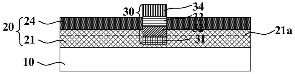
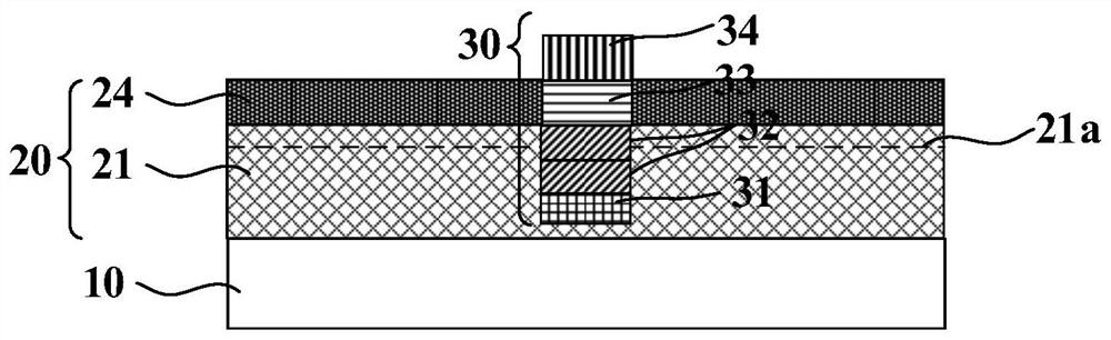
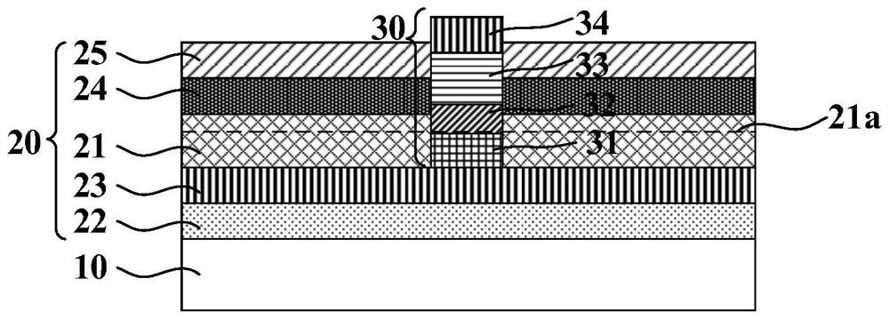
[0026] refer to figure 1 As shown, it is a schematic diagram of a semiconductor device provided by an embodiment of the present invention. The semiconductor device includes: a substrate 10 , an epitaxial multilayer structure 20 formed on the substrate 10 , and a gate structure 30 formed on the epitaxial multilayer structure 20 , and the gate stru...


PUM

PropertyMeasurementUnit
thicknessaaaaaaaaaa
thicknessaaaaaaaaaa
thicknessaaaaaaaaaa

Abstract

Embodiments of the present invention disclose a semiconductor device and a method for manufacturing the same. The semiconductor device includes: a substrate, an epitaxial multilayer structure formed on the substrate, and a gate structure formed on the epitaxial multilayer structure , the gate structure is embedded in the epitaxial multilayer structure, the gate structure sequentially includes a gate channel layer, a gate modulation layer and a gate metal layer, and the material of the gate modulation layer contains aluminum components, and the aluminum component content is variable. The gate modulation layer of the present invention can effectively avoid the problem of increasing on-resistance caused by the height difference between the gate channel layer and the surrounding channel layer, realize the precise control of the threshold voltage of the semiconductor device, and improve the threshold value Voltage uniformity and electron mobility.

Description

technical field [0001] Embodiments of the present invention relate to microelectronic technology, and in particular, to a semiconductor device and a method for manufacturing the same. Background technique [0002] Gallium nitride (GaN)-based semiconductor materials have the characteristics of large band gap, high voltage resistance, high temperature resistance, corrosion resistance and radiation resistance. Moreover, GaN can form a high electron mobility transistor (HEMT) through a heterostructure, which has the advantages of high breakdown voltage, low on-resistance, high switching frequency, and low loss, and is an ideal material for making power devices. GaN HEMTs are classified into enhancement mode and depletion mode according to their different conduction modes. [0003] AlGaN / GaN heterostructures have strong two-dimensional electron gas and high electron mobility, and devices formed by AlGaN / GaN heterojunctions are usually depletion-mode devices. However, the applic...

Claims


Application Information

Patent Timeline
Patent Type & Authority Patents(China)
IPC IPC(8): H01L29/10H01L29/20H01L29/423H01L21/335H01L29/778
CPCH01L29/42316H01L29/1029H01L29/2003H01L29/778H01L29/66462
Inventor 裴轶钱洪途吴星星
Owner DYNAX SEMICON
Why Eureka
Try Eureka