Optical waveguide intensity modulator chip with large optical path difference

An intensity modulator and optical waveguide technology, applied in the directions of light guide, optics, instruments, etc., can solve the problems of insufficient optical power, inability to detect electric field, large difference in the splitting ratio of interference arms, etc., and achieve the effect of increasing the tunable range.

Active Publication Date: 2020-03-27
THE 44TH INST OF CHINA ELECTRONICS TECH GROUP CORP
View PDF5 Cites 2 Cited by
  • Summary
  • Abstract
  • Description
  • Claims
  • Application Information

AI Technical Summary

Problems solved by technology

The bending loss of the waveguide with this structure will increase, resulting in insufficient optical power when measuring a small electric field, the signal strength will be smaller than the noise strength in the system, and the electric field cannot be detected
In addition, the difference in splitting ratio between the two interference arms using this structure is large, which will directly affect the switching extinction ratio of the device.

Method used


Image

  • Optical waveguide intensity modulator chip with large optical path difference
  • Optical waveguide intensity modulator chip with large optical path difference
  • Optical waveguide intensity modulator chip with large optical path difference

Examples


Embodiment Construction

[0025] The present invention will be further described below in conjunction with accompanying drawing.

[0026] In the description of the present invention, unless otherwise specified and limited, it should be noted that the term "connection" should be understood in a broad sense, for example, it can be a mechanical connection or an electrical connection, or it can be the internal communication of two elements, it can be Directly connected or indirectly connected through an intermediary, those skilled in the art can understand the specific meanings of the above terms according to specific situations.

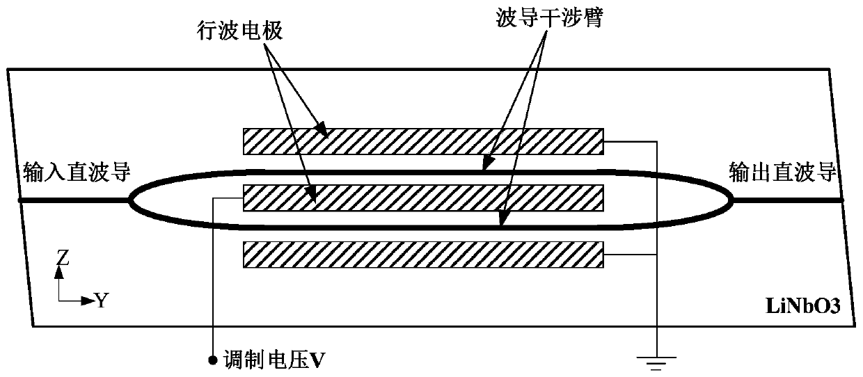
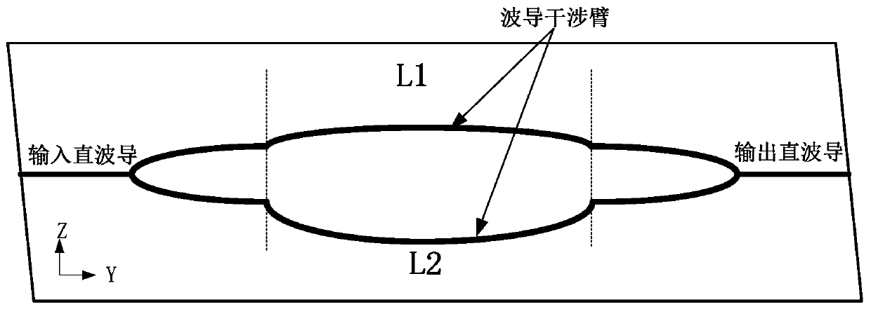
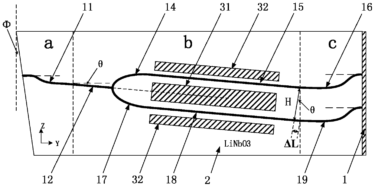
[0027] Such as image 3 As shown, the present invention includes an optical waveguide, a substrate 2 and an electrode 3, and the optical waveguide includes an input end waveguide 11, a Y-shaped branch waveguide, a first interference arm 15, a second interference arm 18, a first output end waveguide 16 and a second waveguide Two output end waveguides 19; the input end waveguide ...


PUM


Abstract

The invention discloses an optical waveguide intensity modulator chip with large optical path difference. The chip comprises an optical waveguide, a substrate and an electrode. The substrate is made of a photoelectric material, and the optical waveguide comprises an input end waveguide, a Y-shaped branch waveguide, a first interference arm, a second interference arm, a first output end waveguide and a second output end waveguide. The arm length of the first interference arm is smaller than that of the second interference arm, transmission shafts of the first interference arm and the second interference arm are straight lines, and included angles between the transmission shafts and a Y axis are theta. A high-reflection film is plated on the end surface of the output end of the chip. According to the invention, an included angle is formed between the two interference arms and the Y axis, so that the two interference arms can form an optical path difference, and the detection sensitivityof the chip and the splitting ratio of the two interference arms are not influenced. The high-reflection film is plated on the end face of the output end of the chip, so that the optical path difference of the light intensity modulator can be doubled, large optical path difference is generated under the condition that the length of the chip is not increased, and the tunable range of the wavelengthis increased.

Description

technical field [0001] The invention relates to the field of optical waveguide intensity modulators, in particular to an optical waveguide intensity modulator chip with a large optical path difference. Background technique [0002] Compared with electrical sensors, optical waveguide intensity modulators have the advantages of high sensitivity, large linear dynamic range, wide frequency response, small size, and little interference to the measured electric field, so they have greater application advantages in the field of electric field sensing. [0003] Such as figure 1 As shown, the traditional optical waveguide intensity modulator, as the core part of the integrated optical sensing test system, adopts the Mach-Zehnder M-Z interferometer structure; Change, so as to modulate the light wave, and complete the detection of electrical signals. [0004] For the integrated optical waveguide intensity modulator, the linear operating point is an important factor affecting its work...

Claims


Application Information

Patent Timeline
Patent Type & Authority Applications(China)
IPC IPC(8): G02B6/125
CPCG02B6/125G02B2006/1204G02B2006/12159
Inventor 华勇富松
Owner THE 44TH INST OF CHINA ELECTRONICS TECH GROUP CORP
Why Eureka
Try Eureka