
Semiconductor laser tube socket for PD die bonding

A technology of semiconductors and lasers, applied in the field of semiconductor laser tube sockets, can solve problems such as silver glue pollution and mismatching specifications, and achieve the effects of avoiding short circuits, increasing output rate, and improving equipment utilization rate

Inactive Publication Date: 2020-03-31
潍坊华光光电子有限公司
View PDF6 Cites 0 Cited by
  • Summary
  • Abstract
  • Description
  • Claims
  • Application Information

AI Technical Summary

Problems solved by technology

The PD positioning groove of the tube base is a traditional groove-shaped structure, which has disadvantages such as mismatching with conventional PD specifications and silver glue pollution.

Method used


Image

  • Semiconductor laser tube socket for PD die bonding
  • Semiconductor laser tube socket for PD die bonding

Examples


Embodiment 1

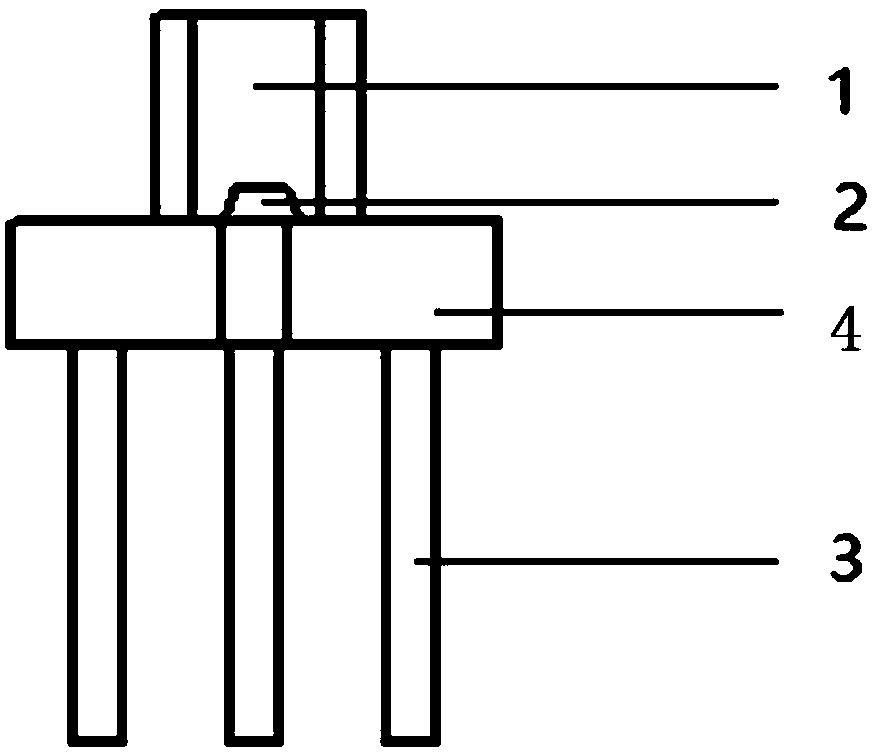
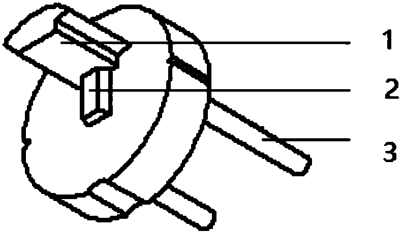
[0019] Such as Figure 1-2 shown.

[0020] A semiconductor laser socket for PD crystal bonding, comprising a main body and a tongue 1 arranged on the upper surface of the main body, a PD area 2 and a PIN pin 3 arranged on the lower surface of the main body; the tongue 1 and the PD area 2 Both are strip structures; the length direction of the tongue 1 is perpendicular to the upper surface of the main body 4, and the length direction of the PD area 2 is parallel to the upper surface of the main body 4; the left and right sides of the PD area 2 are slopes. surface structure. The setting of the slope structure makes the excessive silver glue flow down during the production process to avoid short circuit caused by the silver glue overflowing the PD.

Embodiment 2

[0022] As for the semiconductor laser stem for PD die bonding described in Embodiment 1, further, the length of the PD region 2 is 2200um, the width of the bottom is 700um, and the width of the top is 600um.

Embodiment 3

[0024] For the semiconductor laser tube base for PD die bonding described in Embodiment 1, further, one end of the PD region 2 is connected to the nozzle 1 . It can realize a relatively wide distribution selection range of PD positions, and can realize the selection of the maximum PD current to a characteristic value.


PUM

PropertyMeasurementUnit
Bottom widthaaaaaaaaaa
Top widthaaaaaaaaaa

Abstract

The invention relates to a semiconductor laser tube socket for PD die bonding. The tube socket comprises a main body, a tube tongue arranged on the upper surface of the main body, a PD area and PINs arranged on the lower surface of the main body. The tube tongue and the PD area are both of a strip-shaped structure. The length direction of the tube tongue is perpendicular to the upper surface of the main body, and the length direction of the PD area is parallel to the upper surface of the main body; the left side face and the right side face of the PD area are each of a slope structure. The tube socket can effectively solve the problems of PD failure and equipment stop due to excessive abnormity caused by poor glue amount control; the output rate and the equipment utilization rate are effectively improved, and the marking characteristics of PR recognition are provided for automatic equipment.

Description

technical field [0001] The invention relates to a semiconductor laser socket used for PD crystal solidification, and belongs to the technical field of semiconductor laser production equipment. Background technique [0002] Since its inception in 1962, semiconductor lasers have the advantages of all-solid-state, small size, light weight, long life, high efficiency, high reliability, and high metal-to-semiconductor laser absorption, so they are widely used in pumping of solid-state lasers, laser processing, Laser cutting, precision detection and measurement, communication and information processing, medical treatment and beauty, military and other aspects, and achieved revolutionary breakthroughs in many fields, the market demand and development potential are huge. [0003] Due to the high collimation of laser, it is widely used in communication indication and other fields, among which TO-CAN packaging has become a mature technology in the industry. Usually, TO5.6 packaged la...

Claims


Application Information

Patent Timeline
IPC IPC(8): H01S5/022
CPCH01S5/023H01S5/0233H01S5/02345H01S5/0235
Inventor 张骋梁盼张秀萍汤庆敏
Owner 潍坊华光光电子有限公司
Learn More