
OLED display panel

A display panel and substrate technology, which is applied in the field of OLED display panels, can solve problems such as lack of conductivity, achieve uniform voltage, good stability, and increase the total aperture ratio

Inactive Publication Date: 2020-04-10
SHENZHEN CHINA STAR OPTOELECTRONICS SEMICON DISPLAY TECH CO LTD
View PDF5 Cites 0 Cited by
  • Summary
  • Abstract
  • Description
  • Claims
  • Application Information

AI Technical Summary

Problems solved by technology

However, traditional conductive inks, or carbon-based conductive inks, do not have conductivity themselves. After printing, they need to go through certain post-processing processes such as sintering and annealing to remove solvents, dispersants, stabilizers, etc. in conductive inks. , Only when the conductive material forms a continuous thin film can it have conductivity

Method used


Image

  • OLED display panel
  • OLED display panel
  • OLED display panel

Examples


Embodiment Construction

[0031] The following will clearly and completely describe the technical solutions in the embodiments of the present invention with reference to the drawings in the embodiments of the present invention. Apparently, the described embodiments are only some of the embodiments of the present invention, but not all of them. Based on the embodiments of the present invention, all other embodiments obtained by those skilled in the art without creative efforts fall within the protection scope of the present invention.

[0032] The terms "first", "second", "third", etc. (if any) in the description and claims of the present invention and the above drawings are used to distinguish similar objects and not necessarily to describe a specific order or sequentially. It should be understood that the items so described are interchangeable under appropriate circumstances. Furthermore, the terms "comprising" and "having", as well as any variations thereof, are intended to cover a non-exclusive in...


PUM

PropertyMeasurementUnit
melting pointaaaaaaaaaa

Abstract

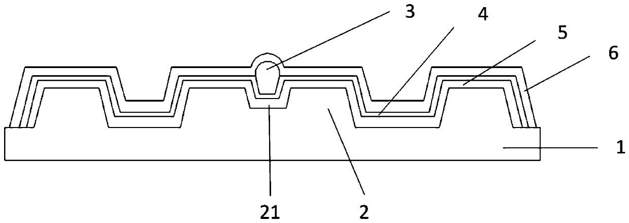
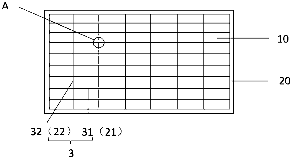
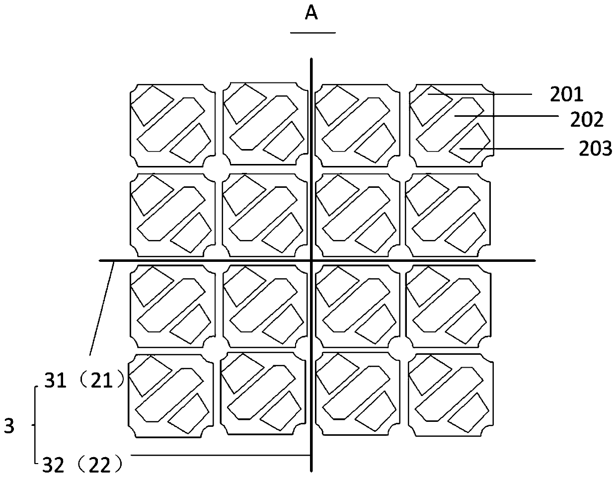
The present invention provides an OLED display panel. The OLED display panel includes: a substrate; a pixel defining layer arranged on the substrate and used for defining pixel units, wherein at leastone first groove extending in the first direction is formed in the side, deviating from the substrate, of the pixel defining layer; and metal components arranged in the at least one first groove, wherein the metal components are electrically connected with a transparent cathode.

Description

technical field [0001] The invention relates to the field of display technology, in particular to an OLED display panel. Background technique [0002] The top-emitting OLED display panel has broad application prospects, but the top-emitting OLED display panel requires a certain high transparency of the top electrode (cathode). If a metal such as magnesium-silver alloy is used as the top electrode, its thickness must be controlled within the range of less than 20nm, but when the metal is so thin, the cross-sectional current is greatly limited, showing poor conductivity. When the cathode is applied to a large-size display panel, the voltage drop (IR Drop) in different areas of the panel will be different due to the different distance from the supply circuit, and the final display area will be uneven. [0003] To solve this problem, the existing method is to add additional metal components in the panel area, in addition to the display pixel area. When preparing the OLED displa...

Claims


Application Information

Patent Timeline
Patent Type & Authority Applications(China)
IPC IPC(8): H01L27/32H01L51/52H01L51/56G09F9/30
CPCG09F9/301H10K59/122H10K50/80H10K50/828H10K71/00H10K50/824H10K2102/3026H10K50/84
Inventor 刘明
Owner SHENZHEN CHINA STAR OPTOELECTRONICS SEMICON DISPLAY TECH CO LTD
Learn More