Micro-led array device based on Group III nitride semiconductor and its preparation method

A technology of nitride semiconductors and arrays, applied in semiconductor devices, electrical solid devices, electrical components, etc., can solve optical crosstalk, can not solve optical crosstalk, and silver cannot be used as electrodes, etc., to improve luminous efficiency and increase current expansion range , Solve the effect of mutual crosstalk

Active Publication Date: 2020-12-01
NANJING UNIV
View PDF1 Cites 0 Cited by
  • Summary
  • Abstract
  • Description
  • Claims
  • Application Information

AI Technical Summary

Problems solved by technology

However, such isolation grooves cannot block the transmission of light, so there is still the problem of optical crosstalk between adjacent pixel units
The role of silver filling is to enhance the quantum efficiency of LED devices through silver metal, and it cannot solve the problem of optical crosstalk. At the same time, the filled silver cannot be used as an electrode

Method used


Image

  • Micro-led array device based on Group III nitride semiconductor and its preparation method
  • Micro-led array device based on Group III nitride semiconductor and its preparation method
  • Micro-led array device based on Group III nitride semiconductor and its preparation method

Examples


Embodiment 1

[0054] The preparation method of the Micro-LED array device based on III-nitride semiconductor with barrier added, the steps include:

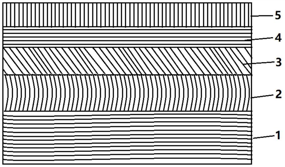
[0055] This method is processed on the Si blue light LED epitaxial wafer, and the structure of the Si blue light LED epitaxial wafer is:

[0056] A Si substrate 1 with a thickness of 800 μm;

[0057] A GaN buffer layer 2 grown on the Si substrate, with a thickness of 1750nm;

[0058] An n-type GaN layer 3 grown on the buffer layer with a thickness of 1650nm;

[0059] An InGaN / GaN quantum well active layer 4 grown on an n-type GaN layer; the thickness of the InGaN / GaN quantum well active layer is 200nm, the number of periods is 10, the In content is 0.26, the Ga content is 0.74, and the well width is 2.2nm, the barrier thickness is 5.8nm;

[0060] A p-type GaN layer 5 grown on the quantum well active layer with a thickness of 100 nm.

[0061] (1) Using PECVD (Plasma Enhanced Chemical Vapor Deposition) technology to evaporate a layer of 150n...

Embodiment 2

[0072] The preparation method of the Micro-LED array device based on III-nitride semiconductor with barrier added, the steps include:

[0073] This method is processed on the Si blue light LED epitaxial wafer, and the structure of the Si blue light LED epitaxial wafer is:

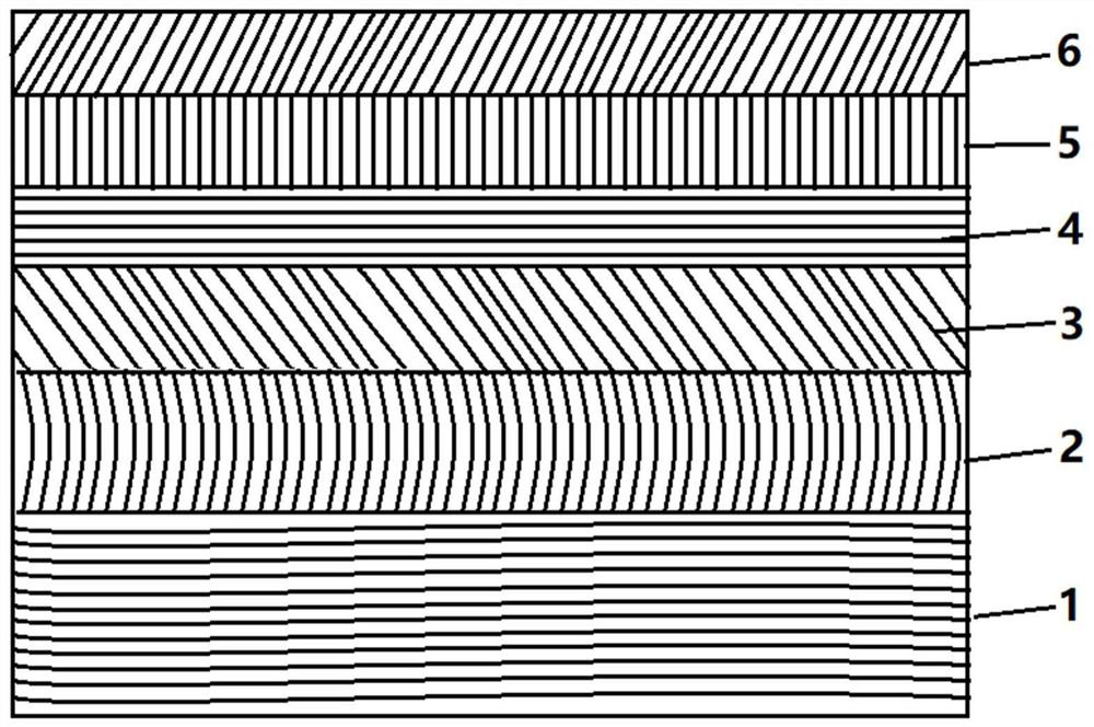
[0074] A Si substrate 1 with a thickness of 800 μm;

[0075] A GaN buffer layer 2 grown on the Si substrate, with a thickness of 1750nm;

[0076] An n-type GaN layer 3 grown on the buffer layer with a thickness of 1750nm;

[0077] An InGaN / GaN quantum well active layer 4 grown on an n-type GaN layer; the thickness of the InGaN / GaN quantum well active layer is 250nm, the number of periods is 10, the In content is 0.26, the Ga content is 0.74, and the well width is 2.2nm, the barrier thickness is 5.8nm;

[0078] A p-type GaN layer 5 grown on the quantum well active layer with a thickness of 150nm.

[0079] (1) Using PECVD (plasma enhanced chemical vapor deposition) technology to evaporate a layer of 200nm t...

Embodiment 3

[0090] The preparation method of the Micro-LED array device based on III-nitride semiconductor with barrier added, the steps include:

[0091] This method is processed on the Si blue light LED epitaxial wafer, and the structure of the Si blue light LED epitaxial wafer is:

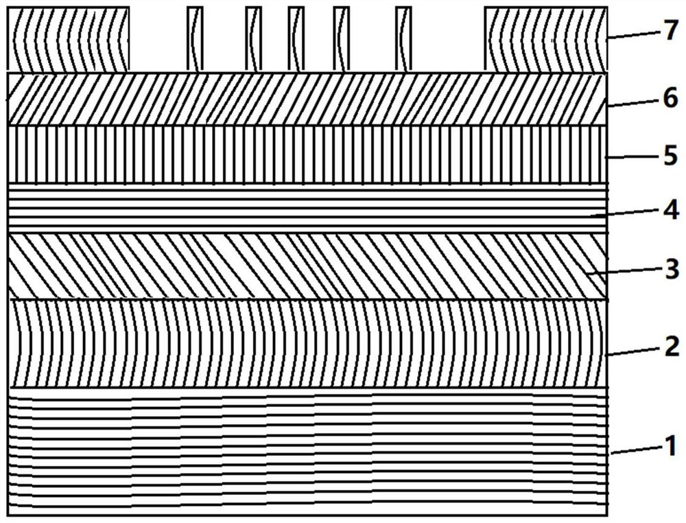
[0092] A Si substrate 1 with a thickness of 800 μm;

[0093] A GaN buffer layer 2 grown on the Si substrate, with a thickness of 1750nm;

[0094] An n-type GaN layer 3 grown on the buffer layer with a thickness of 1850nm;

[0095] An InGaN / GaN quantum well active layer 4 grown on an n-type GaN layer; the thickness of the InGaN / GaN quantum well active layer is 300nm, the number of periods is 10, the In content is 0.26, the Ga content is 0.74, and the well width is 2.2nm, the barrier thickness is 5.8nm;

[0096] A p-type GaN layer 5 grown on the quantum well active layer with a thickness of 200nm.

[0097] (1) Using PECVD (plasma enhanced chemical vapor deposition) technology to evaporate a layer of 250nm...


PUM

PropertyMeasurementUnit
thicknessaaaaaaaaaa
thicknessaaaaaaaaaa
thicknessaaaaaaaaaa

Abstract

The invention discloses a Micro-LED array device based on group III nitride semiconductors, which is etched to form an array fan-shaped mesa structure that penetrates the p-type GaN layer, the quantum well active layer, and reaches the n-type GaN layer, and the p-type array The electrodes are vapor-deposited on the p-type GaN layer of the fan-shaped array, and the n-type array electrodes are vapor-deposited on the n-type GaN layer, and the n-type array electrodes form barriers to isolate the fan-shaped mesas from each other. And discloses its preparation method. In the present invention, a retaining wall made of n-type electrodes is added between the light-emitting units of the Micro-LED fan-shaped table array. The problem of crosstalk between units is beneficial to realize individual control; the use of n-type electrode metal as a retaining wall and the use of p-type electrodes with a mesh structure increases the current expansion range and effectively improves luminous efficiency.

Description

technical field [0001] The invention relates to a Micro-LED array device based on Group III nitride semiconductors and a preparation method thereof, belonging to the technical field of semiconductor lighting and display. Background technique [0002] Group III nitride materials, as direct bandgap semiconductors, cover a wide spectral range from deep ultraviolet to near infrared, and have achieved great success in realizing high-efficiency solid-state lighting and ultra-high-resolution displays. Different from traditional lighting methods, semiconductor lighting is a revolutionary technology. It uses semiconductor chips as light sources to directly convert electrical energy into light energy, so the conversion efficiency is relatively high. As the core component of solid-state lighting semiconductor light source, light-emitting diode (LED) has the advantages of high brightness, long life, small size, low energy consumption, green environmental protection, safe use, etc., and ...

Claims


Application Information

Patent Timeline
Patent Type & Authority Patents(China)
IPC IPC(8): H01L33/38H01L33/06H01L33/00H01L33/20
CPCH01L33/007H01L33/06H01L33/382H01L33/20H01L33/32H01L27/156H01L25/0753H01L33/0025H01L33/0075H01L33/24H01L33/40
Inventor 陶涛王轩许非凡刘斌智婷张荣
Owner NANJING UNIV
Why Eureka
Try Eureka