Drive control circuit and method for optimizing switching characteristics of power semiconductor device

A technology for driving control circuits and power semiconductors, applied in electronic switches, program control, general control systems, etc., can solve problems such as high switching speed, voltage and current shock, waveform oscillation, etc., to reduce voltage and current spikes, protect safety, reduce Effect of Oscillation Time

Pending Publication Date: 2020-04-10
GLOBAL ENERGY INTERCONNECTION RES INST CO LTD
View PDF1 Cites 3 Cited by
  • Summary
  • Abstract
  • Description
  • Claims
  • Application Information

AI Technical Summary

Problems solved by technology

[0003] In view of this, the embodiment of the present invention provides a driving control circuit and method for optimizing the switching characteristics of power semiconductor devices, which solves the problems of obvious voltage and current impact and waveform oscillation caused by excessive switching speed in the prior art

Method used


Image

  • Drive control circuit and method for optimizing switching characteristics of power semiconductor device
  • Drive control circuit and method for optimizing switching characteristics of power semiconductor device
  • Drive control circuit and method for optimizing switching characteristics of power semiconductor device

Examples


Embodiment 1

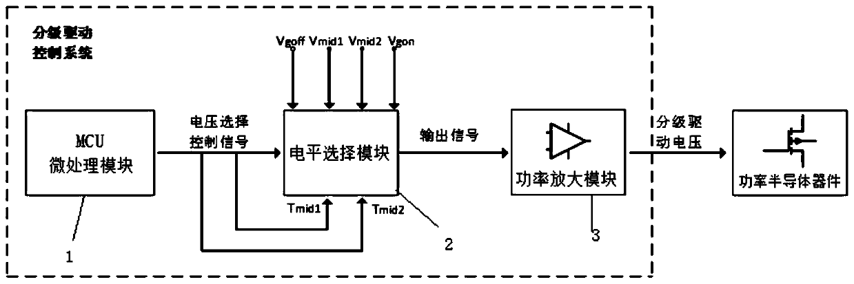
[0027] An embodiment of the present invention provides a drive control circuit that optimizes the switching characteristics of a power semiconductor device, such as figure 1 shown, including:

[0028] The micro-processing module 1 is used for generating driving signals. In the embodiment of the present invention, the micro-processing module 1 generates the drive signal through the MCU micro-control unit, wherein the MCU micro-control unit properly reduces the frequency and specifications of the central processing unit, and uses memory (memory), counter (Timer), Peripheral interfaces such as USB, A / D conversion, UART, PLC, DMA, and even LCD drive circuits are integrated on a single chip to form a chip-level computer, which can be used for different combination controls for different applications. It should be noted that, in the embodiment of the present invention, only the MCU micro-control unit is used as an example for illustration. In practical applications, other micro-con...

Embodiment 2

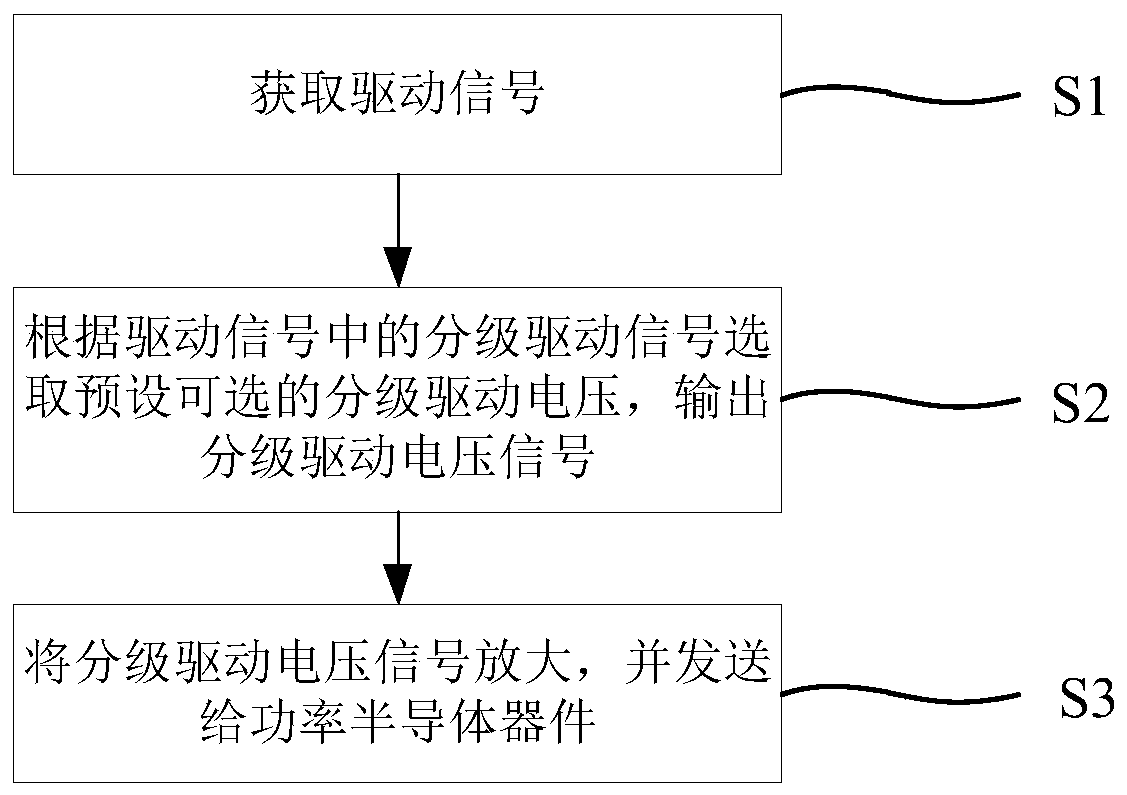
[0033] An embodiment of the present invention provides a driving control method for optimizing the switching characteristics of a power semiconductor device, such as figure 2 As shown, the drive control method for optimizing the switching characteristics of power semiconductor devices includes:

[0034] Step S1: Obtain a driving signal.

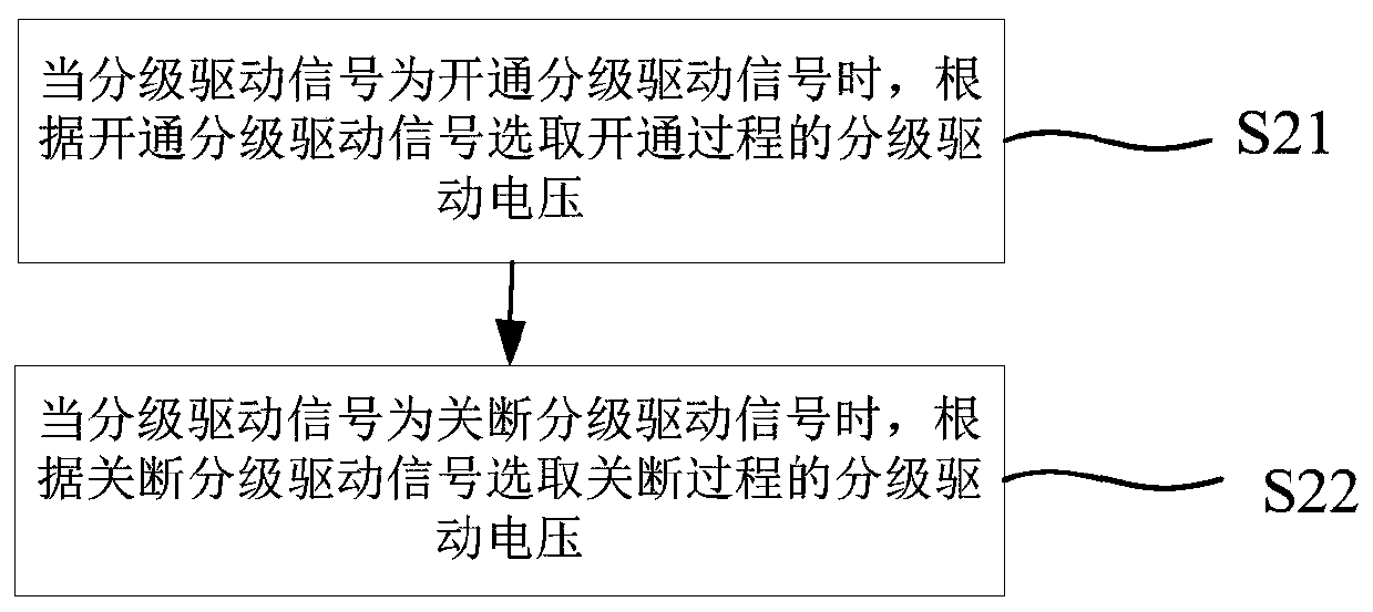
[0035] In the embodiment of the present invention, the driving signal can be generated by the MCU micro-control unit to control the voltage classification, reduce the instantaneous voltage and current amplitude and the noise transmitted to the output and input terminals, thereby reducing electromagnetic interference, wherein the classification driving voltage includes: opening It should be noted that in the embodiment of the present invention, only the MCU micro-control unit is used as an example for illustration. In practical applications, other microcontrollers can also be used to generate the drive signal. The present invention It is not...


PUM


Abstract

The invention discloses a driving control circuit and method for optimizing switching characteristics of a power semiconductor device. The method comprises the following steps: acquiring a driving signal; selecting a preset selectable hierarchical driving voltage according to a hierarchical driving signal in the driving signals, and outputting a hierarchical driving voltage signal; and amplifyingthe graded driving voltage signal and sending the amplified graded driving voltage signal to a power semiconductor device. According to the drive control circuit and method for optimizing switching characteristics of a power semiconductor device, the driving control is taken as an entry point, the graded driving voltage is selected according to the graded driving signal, the graded driving voltagesignal is output and then sent to the power semiconductor device, so that the power semiconductor device makes a corresponding action response, the purpose of optimizing switching characteristics isachieved, and the design difficulty of driving protection is reduced.

Description

technical field [0001] The invention relates to the field of power electronics technology and control technology, in particular to a drive control circuit and method for optimizing switching characteristics of power semiconductor devices. Background technique [0002] As a new type of third-generation power semiconductor device with wide and tight band, SiC MOSFET can greatly reduce the number of cascaded power modules, simplify the topology of the system, and reduce the size of power electronics when used in high-voltage and large-capacity power electronic devices in power systems. The weight, footprint and capacity of the device can be reduced, thereby improving the power density and efficiency of the device. However, in the switching process of SiC MOSFET, the high turn-on and turn-off speed will lead to obvious voltage and current impact, waveform oscillation, electromagnetic interference and other problems, which seriously affect the safety and reliability of power syst...

Claims


Application Information

Patent Timeline
Patent Type & Authority Applications(China)
IPC IPC(8): H03K17/687
CPCH03K17/687G05B2219/25257
Inventor 董振邦徐云飞李卫国邓占锋卢娟娟郝一卜宪德刘海军周哲
Owner GLOBAL ENERGY INTERCONNECTION RES INST CO LTD
Why Eureka
Try Eureka