Pixel compensation circuit of AMOLED

A compensation circuit and pixel technology, applied in the field of pixel compensation circuit, can solve problems such as uneven brightness among pixels, achieve the effect of promoting large-scale mass production and improving display quality

Inactive Publication Date: 2020-04-17
WUHAN CHINA STAR OPTOELECTRONICS SEMICON DISPLAY TECH CO LTD
View PDF11 Cites 1 Cited by
  • Summary
  • Abstract
  • Description
  • Claims
  • Application Information

AI Technical Summary

Problems solved by technology

[0005] The purpose of the present invention is to provide a pixel comp

Method used


Image

  • Pixel compensation circuit of AMOLED
  • Pixel compensation circuit of AMOLED
  • Pixel compensation circuit of AMOLED

Examples


Example Embodiment

[0029] In order to make the objectives, technical solutions, and effects of the present invention clearer and clearer, the present invention will be further described in detail below with reference to the accompanying drawings. It should be understood that the specific embodiments described herein are only used to explain the present invention, and the word "embodiment" used in the specification of the present invention is meant to serve as an example, example or illustration, and is not intended to limit the present invention.

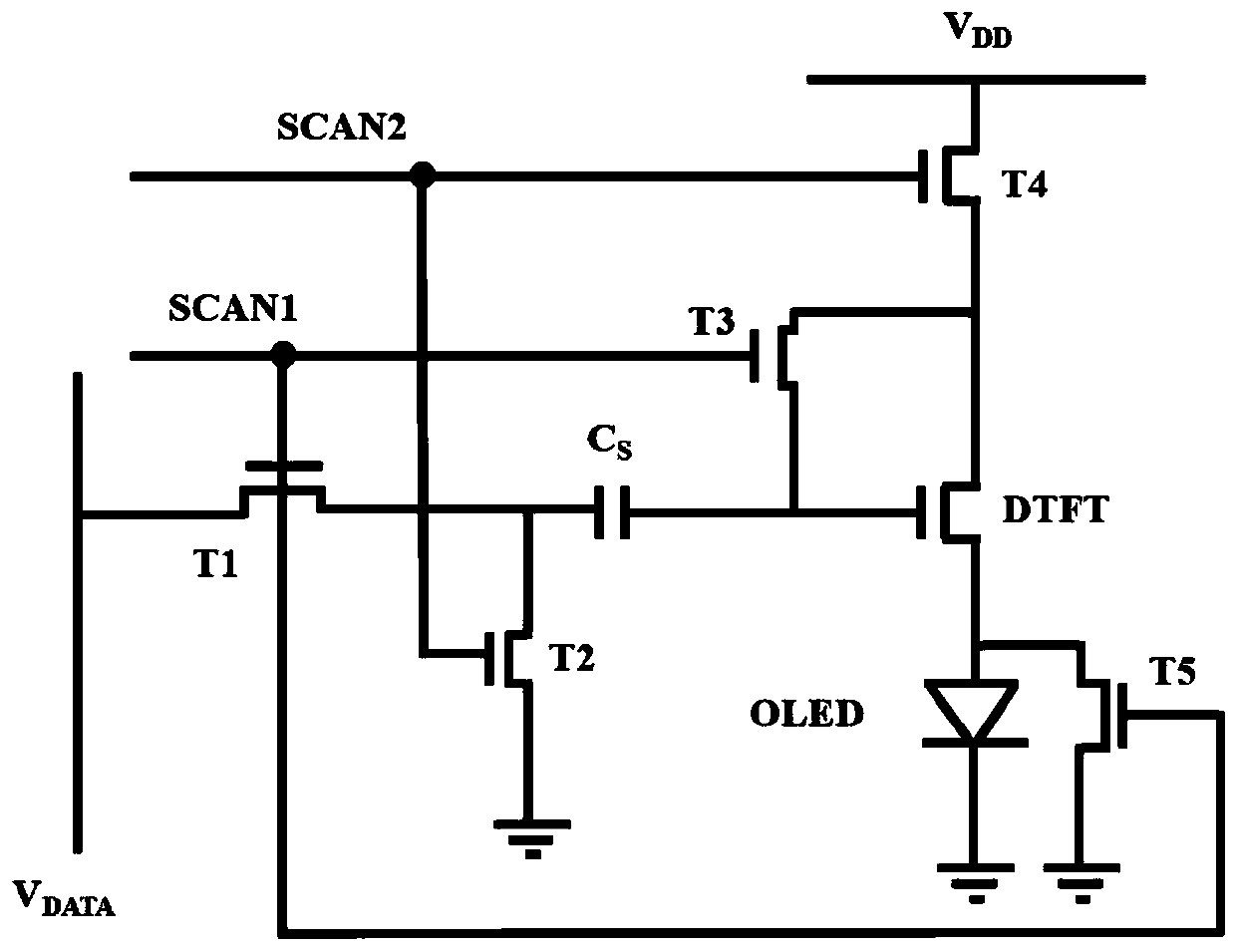
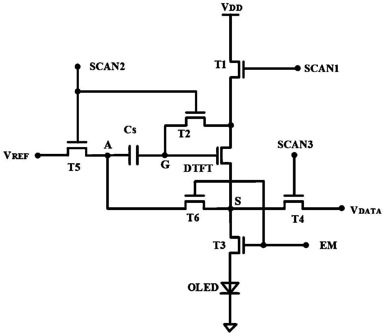
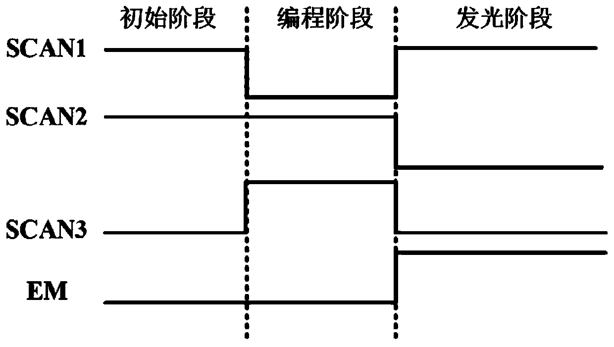
[0030] The present invention provides an AMOLED pixel compensation circuit, which has the effect of solving the poor quality of AMOLED panels caused by uneven brightness between pixels, and aims to make the threshold voltage V TH And OLED anode voltage V OLED Does not affect the luminous current of the display panel.

[0031] Please refer to figure 2 , figure 2 It is a schematic diagram of a pixel compensation circuit in an embodiment of the present inve...


PUM


Abstract

The invention provides a pixel compensation circuit. The pixel compensation circuit comprises seven switches, a storage capacitor, an organic light emitting diode, four signal sources and three inputvoltages. The time sequence of the four signal sources can be divided into an initial stage, a programming stage and a light emitting stage in sequence. Through the matching with the timing sequence high and low levels of the four signal sources, the current flowing through the organic light emitting diode in the light emitting stage of the display is not influenced by the threshold voltage and the anode voltage of the OLED, the drifting of the threshold voltage is effectively compensated, and the problems of uneven brightness and aging of the display panel are further improved.

Description

technical field [0001] The present application relates to an active-matrix organic light emitting diode (AMOLED) display panel, in particular to a pixel compensation circuit of the AMOLED. Background technique [0002] Active Organic Light Emitting Diode (AMOLED) is a current-mode device, which has extremely high requirements on the stability and uniformity of the backplane technology. At present, the backplane technology used in AMOLED mainly includes polysilicon and metal oxide thin film transistors, but because these thin film transistors have a threshold voltage (V TH ) drift, so the current flowing through each pixel is different, causing the problem of uneven brightness among pixels. Furthermore, the OLED panel is likely to cause aging of the AMOLED panel under long-time operation. [0003] refer to figure 1 , figure 1 It is a schematic diagram of a pixel compensation circuit in the prior art. Its structure is composed of five thin film transistors and a storage c...

Claims


Application Information

Patent Timeline
IPC IPC(8): G09G3/3225
CPCG09G3/3225
Inventor 王兰兰李骏
Owner WUHAN CHINA STAR OPTOELECTRONICS SEMICON DISPLAY TECH CO LTD
Why Eureka
Try Eureka